The AI Hardware Stack Is Being Rebuilt From the Wafer Up
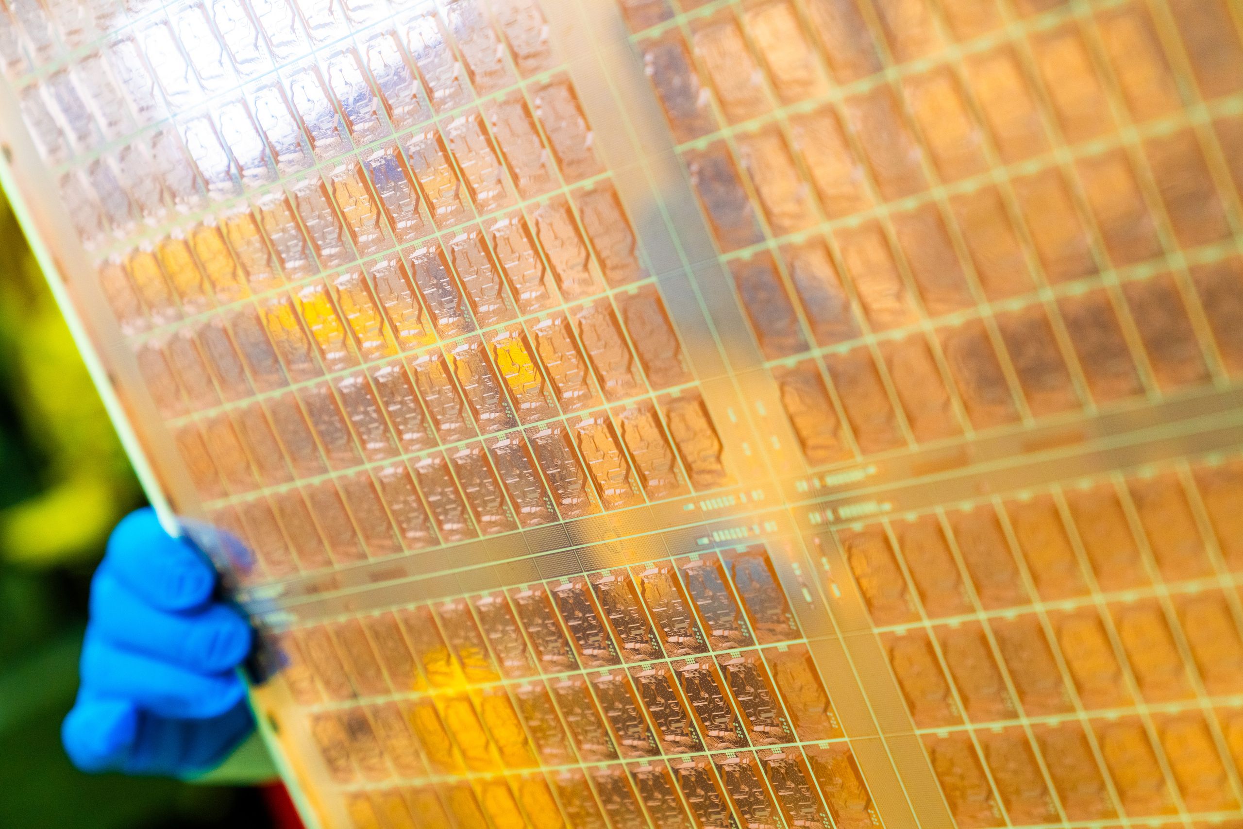
Before a single H100 ever runs a training job, it has to survive one of the most constrained supply chains in industrial history. Every serious AI accelerator, H100, B200, Cerebras WSE-3, starts its life on a TSMC wafer, gets etched by an ASML EUV machine, and then waits in a queue for CoWoS packaging capacity that is sold out through 2026. Understanding that stack matters if you are building on top of it, because the constraints at the bottom determine what compute costs, what latency looks like, and which architectural bets actually pay off.
The Factory Floor Nobody Talks About
TSMC holds 72% of advanced chip manufacturing. That is not a market share number you diversify around quickly. And ASML sits underneath that with a near-monopoly on EUV lithography, the machines that print sub-5nm features. No ASML machines means no advanced chips, full stop. Every H100 and B200 in existence ran through both companies.
But the real chokepoint right now is not transistors. It is CoWoS packaging, the process that physically stacks High Bandwidth Memory next to the compute die on a shared substrate. HBM is what gives these chips their memory bandwidth, and without CoWoS you cannot build them. That packaging capacity is sold out through 2026. TSMC is spending $52-56 billion in capex in 2026 alone, with 70-80% going toward advanced nodes, and it is still not enough to clear the queue.