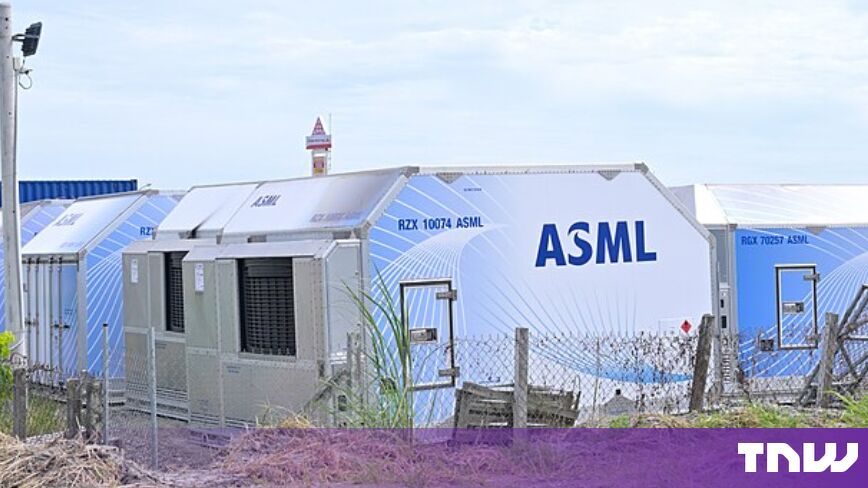
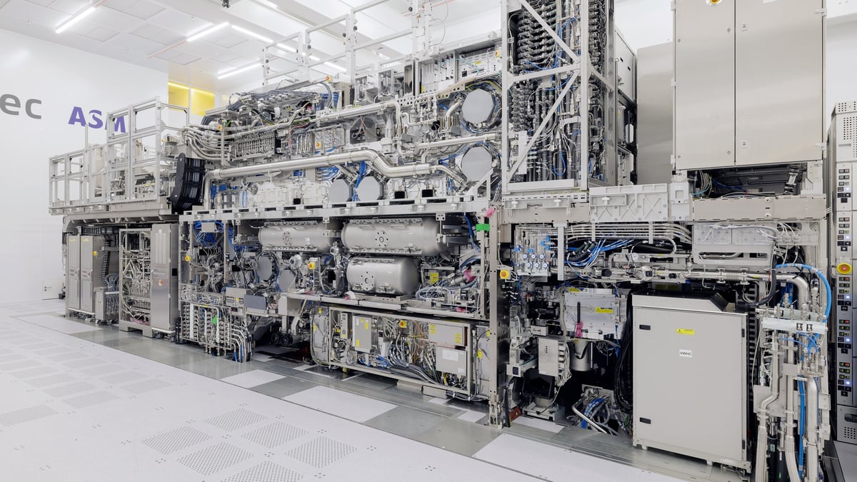
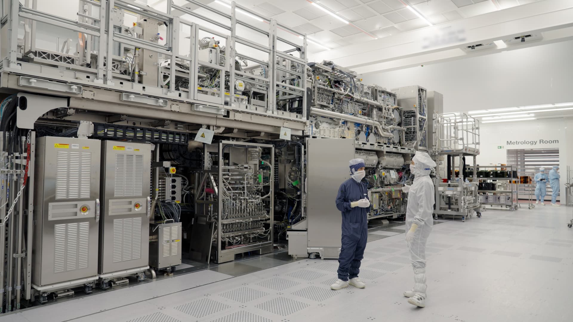
ASML, Intel, Samsung, and TSMC are teaming up to drive the industry transition to 6×12-inch photomasks (reticles). This shift is paramount for High-NA EUV lithography, as the larger stencil would enable printing large chips in a single pass, instead of having to stitch smaller designs together, as ASML explained in a press release this week.This kind of collaboration between chipmakers isn't entirely unheard of, but it is rare. But when they face an industry-wide challenge, they set aside their rivalry and join forces to move the industry forward. This happened several times in recent decades, first with the failed transition to 450-mm wafers co-funded by GlobalFoundries, IBM, Intel, Samsung, TSMC, and New York State, then with the EUV transition, which was spearheaded by Intel, TSMC, and Samsung.
TSMC, Samsung, and Intel shore up support with ASML to deploy larger High-NA EUV photomasks — 6×12-inch photomask transition may take years despite unified effort
ASML, Intel, Samsung, and TSMC back development of 6×12-inch to build large processors using High-NA EUV lithography systems without stitching.
127 words~1 min read