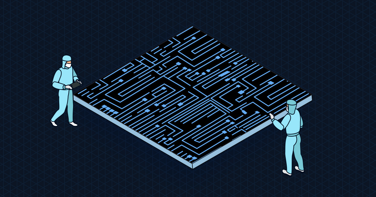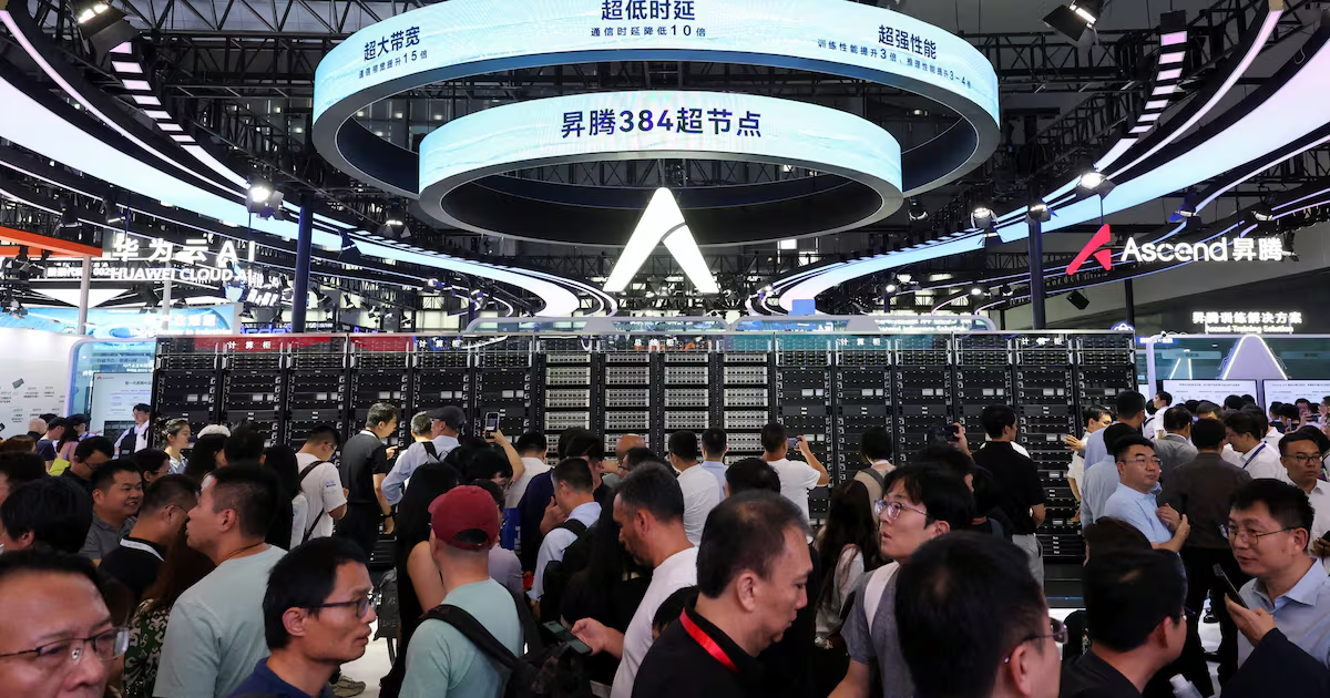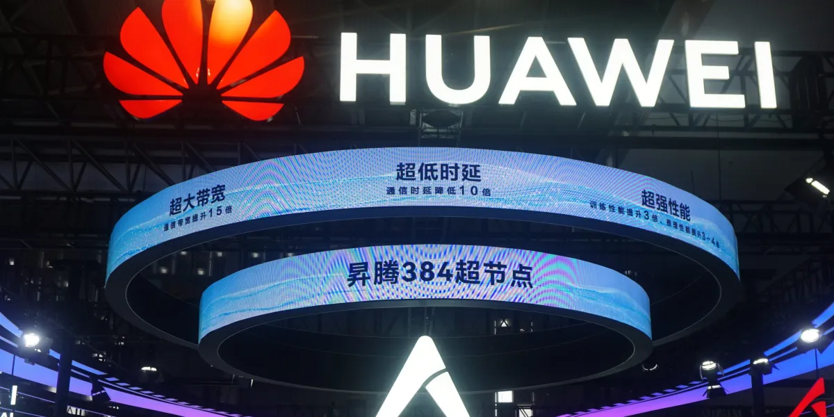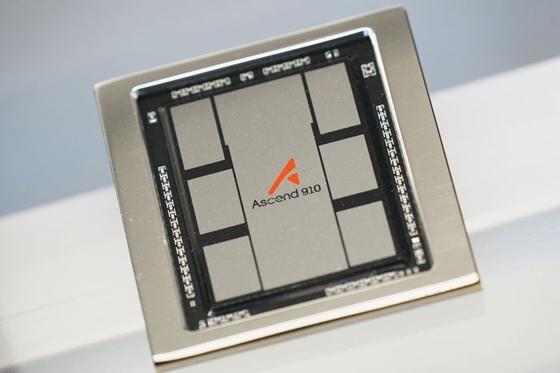
Huawei, through its chip design arm HiSilicon and manufacturing partner Semiconductor Manufacturing International Corp. (SMIC), is targeting production of roughly 600,000 Ascend 910C AI accelerator chips in 2026. That would represent a doubling of previous output levels, part of a broader ambition to churn out 1.6 million chips despite persistent yield challenges and memory constraints.
The company recently unveiled two concepts that signal its strategic direction: the “Tau Scaling Law” and “LogicFolding” architecture. Both prioritize advanced packaging and efficient data movement over the geometric scaling that has defined the semiconductor industry for decades. The company claims this approach could achieve transistor densities comparable to a 1.4nm process by 2031, all without relying on the restricted foreign lithography tools that Washington has tried to keep out of Chinese hands.
Thermal management and power efficiency are significant hurdles that grow exponentially harder as you pack more transistors into tighter spaces, regardless of how you arrange them.
DeepSeek has placed an order for at least 160,000 next-generation Ascend 950DT accelerators, slated for deployment in a 1-gigawatt data center by late 2027 or early 2028.