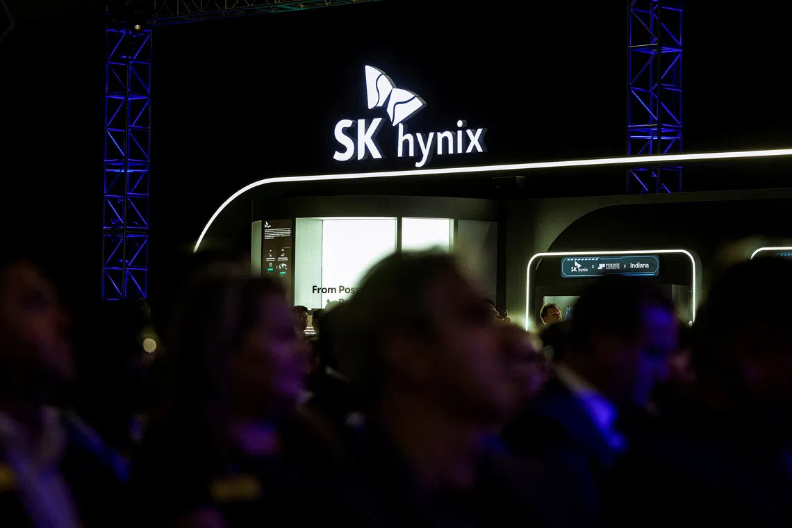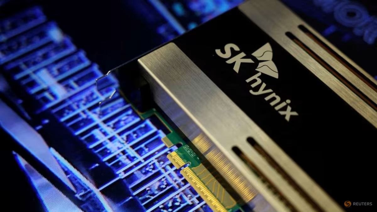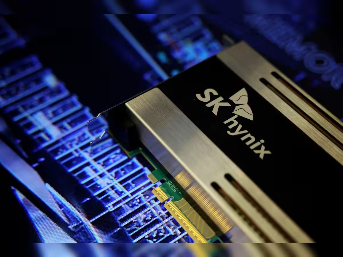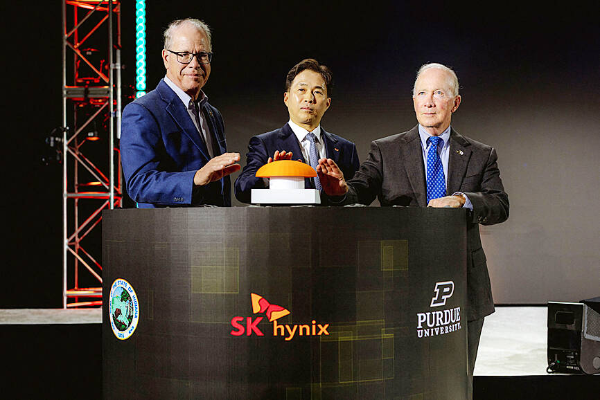
SK Hynix broke ground on a sprawling semiconductor facility in West Lafayette, Indiana on August 27, marking the company’s first manufacturing footprint on American soil. The project, now valued at over $4 billion, will focus on packaging high-bandwidth memory (HBM) chips designed specifically for artificial intelligence workloads.
It’s the largest single development project in Indiana’s history. And it’s being built, quite literally, in Purdue University’s backyard.
What SK Hynix is building
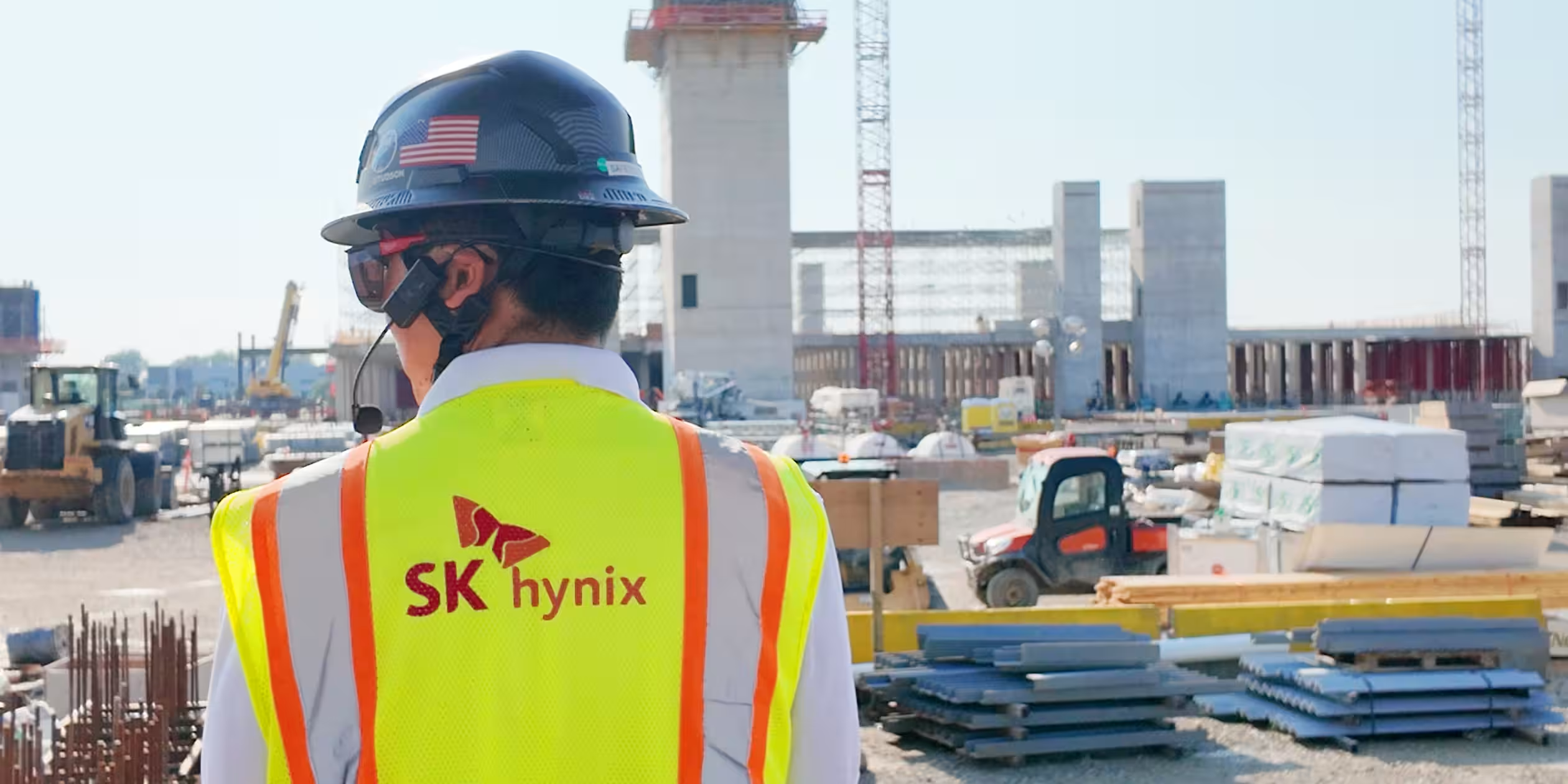
The facility sits on a 133.5-acre site at Purdue Research Park, where foundation and piling work has been underway since early 2026. The groundbreaking ceremony formalized what construction crews have been doing for months.
Cleanroom operations, where the actual chip packaging will happen, are expected to come online in the second half of 2028.