DOMESTIC CHIPS:
The CEO said that when fully operational, the facility, which has US CHIPS Act funding, would be a major HBM hub employing about 1,000 people
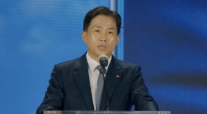
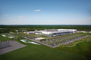
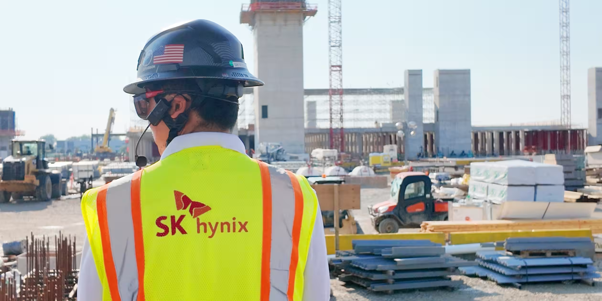
SK Hynix Inc on Thursday held a groundbreaking ceremony for its advanced memory packaging facility in Indiana, marking a milestone in Washington’s expansive campaign to rebuild domestic supply chains and manufacturing for strategically important sectors.The West Lafayette plant, costing more than US$4 billion and occupying a 54-hectare site, is to be SK Hynix’s first high-bandwidth memory (HBM) packaging base in the US. Its cleanroom is expected to open by October 2028, with mass production of next-generation HBM scheduled to begin in the second half of 2029, chief executive officer Kwak Noh-jung said at the event.When fully operational, it would be a major HBM hub employing about 1,000 people, Kwak said.
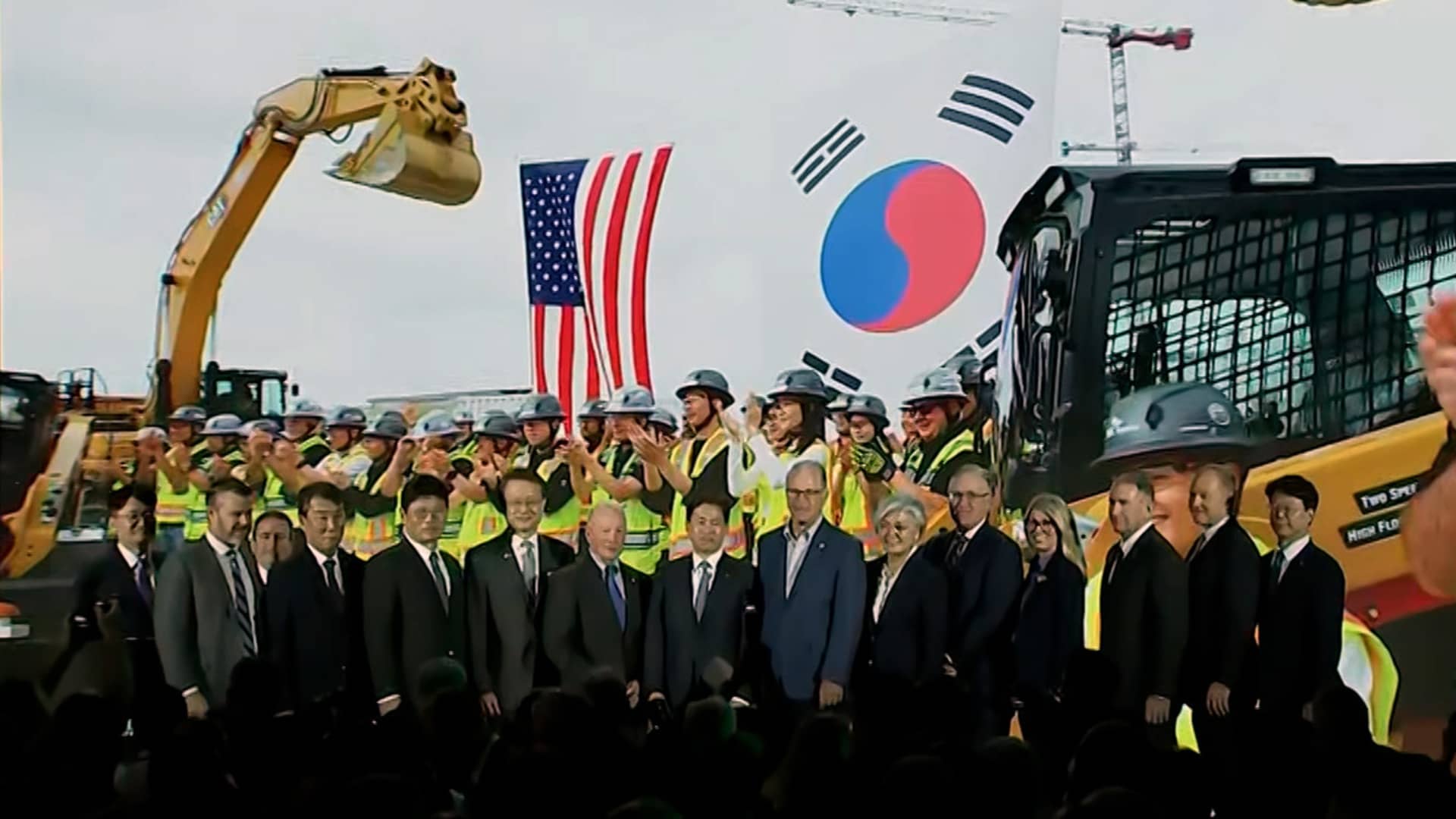
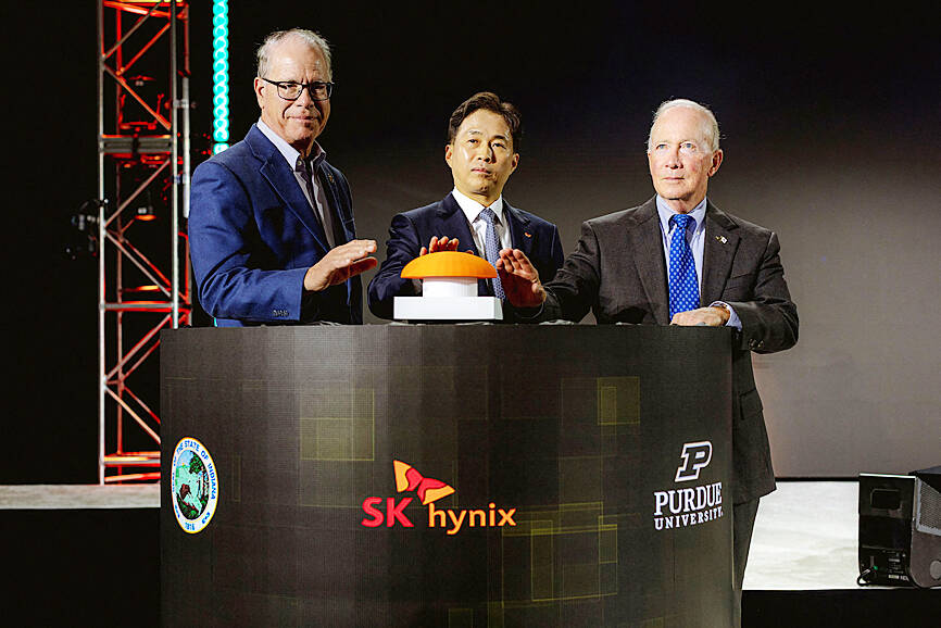
Indiana Governor Mike Braun, SK Hynix president and chief executive officer Kwak Noh-jung and Purdue University president Mitchell Daniels Jr wait to press a button to begin construction at a groundbreaking ceremony in West Lafayette, Indiana, on Thursday.
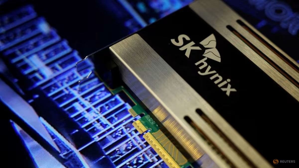
HBM is an indispensable part of the global artificial intelligence (AI) hardware boom, as it is prerequisite for assembling Nvidia Corp’s most advanced AI acceleration systems.That has helped SK Hynix grow to become South Korea’s second-most valuable company, behind Samsung Electronics Co, which has also been lifted by runaway demand for HBM and other memory products.