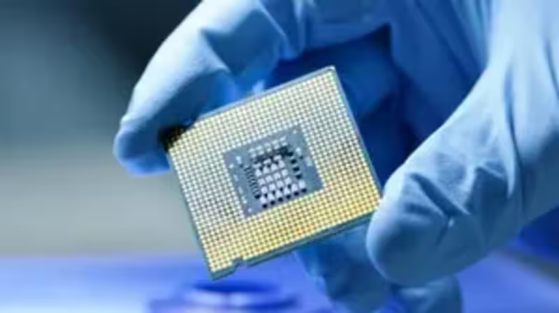
Intel is going all-in on the most expensive piece of equipment in semiconductor history. The chipmaker has adopted ASML’s next-generation High-NA EUV lithography system, a tool that costs roughly $400 million per unit, to power its future laptop chip production and broader processor roadmap.
The $400 million machine
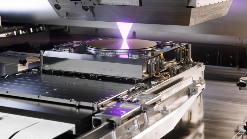
High-NA EUV, which stands for high numerical aperture extreme ultraviolet lithography, is the latest leap in the ongoing miniaturization race. It uses incredibly precise light to draw circuit patterns at scales that eliminate the need for multiple patterning steps, which slow production and drive up defect rates.
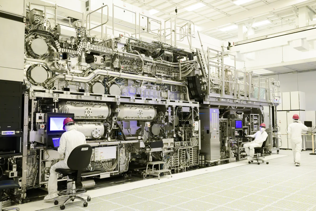
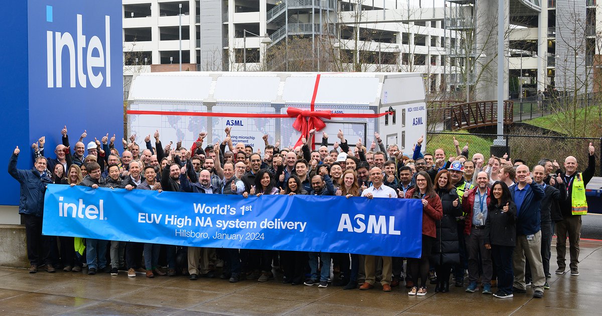
Intel installed the industry’s first commercial High-NA EUV scanner, ASML’s TWINSCAN EXE:5000, at its Oregon R&D fab in April 2024. By late 2025, the company advanced to the more production-ready EXE:5200B model, which is expected to achieve throughput of over 175 wafers per hour.
ASML confirmed in February 2026 that its High-NA EUV tools are ready for high-volume manufacturing. The company reported processing 500,000 wafers with approximately 80% uptime, a benchmark that cleared the path for commercial deployment.