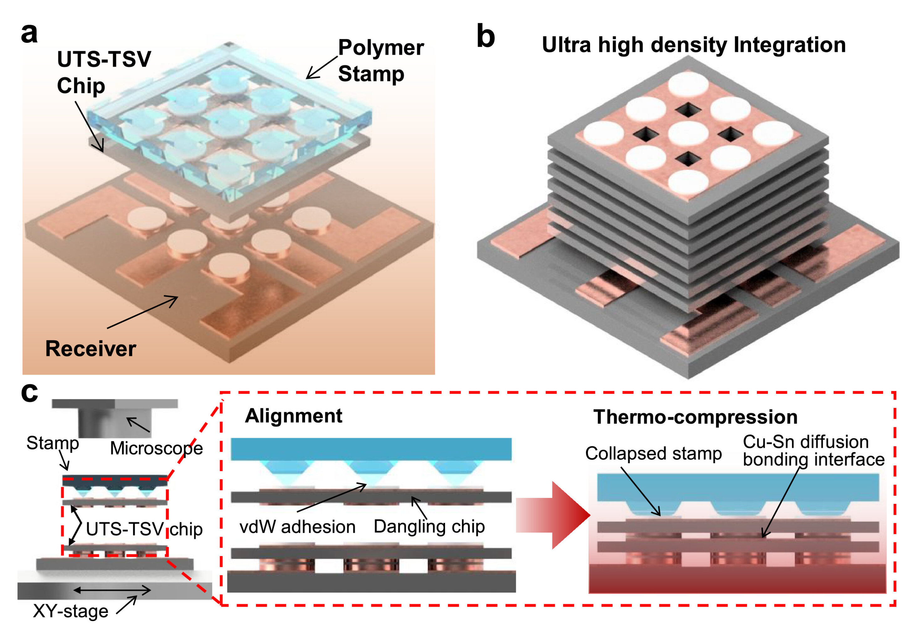
Transfer printing and in-situ bonding concept. a) Overall schematic. b) Ultra-high-density integration schematic. c) Conceptual model of transfer printing and in-situ bonding based integration. Credit: Results in Engineering (2026). DOI: 10.1016/j.rineng.2026.111194
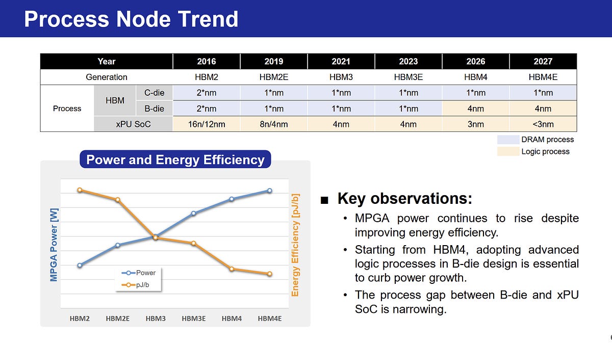
A Korean research team has developed a technology that enables the stable stacking of more than 10 ultrathin semiconductor chips, each only one-fifth the thickness of a human hair. A research team successfully achieved an integration density approximately four times higher than that of commercial high-bandwidth memory (HBM) through a novel process that simultaneously transfers chips and forms metallic interconnections. The study was published in the journal Results in Engineering. The team was led by Prof. Seok Kim and integrated Ph.D. student Uhyeon Kim from the Department of Mechanical Engineering at POSTECH (Pohang University of Science and Technology), together with Dr. Hohyun Keum of the Korea Institute of Industrial Technology (KITECH).
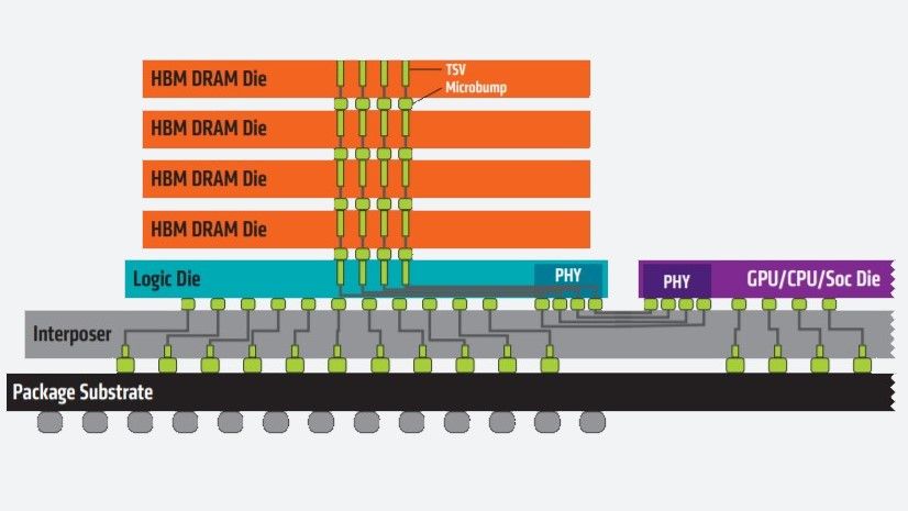
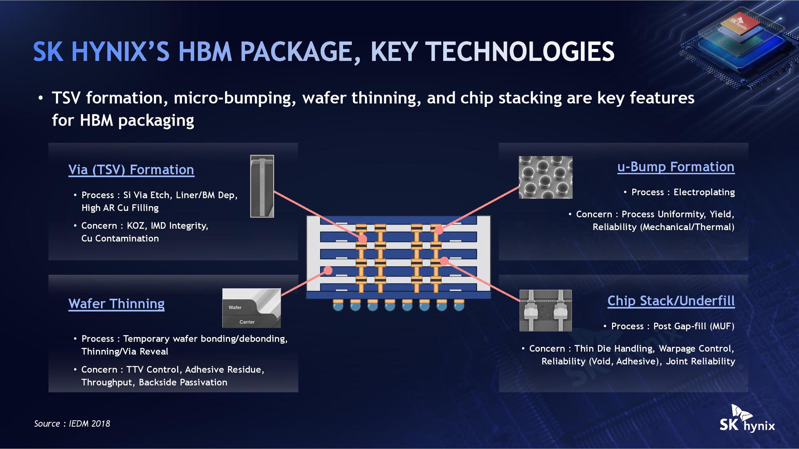
AI services such as ChatGPT, image-generation AI and autonomous vehicles share one common requirement: they must process enormous amounts of data at extremely high speeds. While electronic devices continue to become thinner, semiconductor performance continues to improve because chips are no longer expanded laterally but stacked vertically. This is analogous to constructing high-rise apartment buildings instead of single-family homes when urban land becomes scarce. High-bandwidth memory (HBM), a key technology that determines the performance of AI accelerators, is built by vertically stacking multiple memory chips, making the ability to reliably stack a large number of chips a critical challenge.