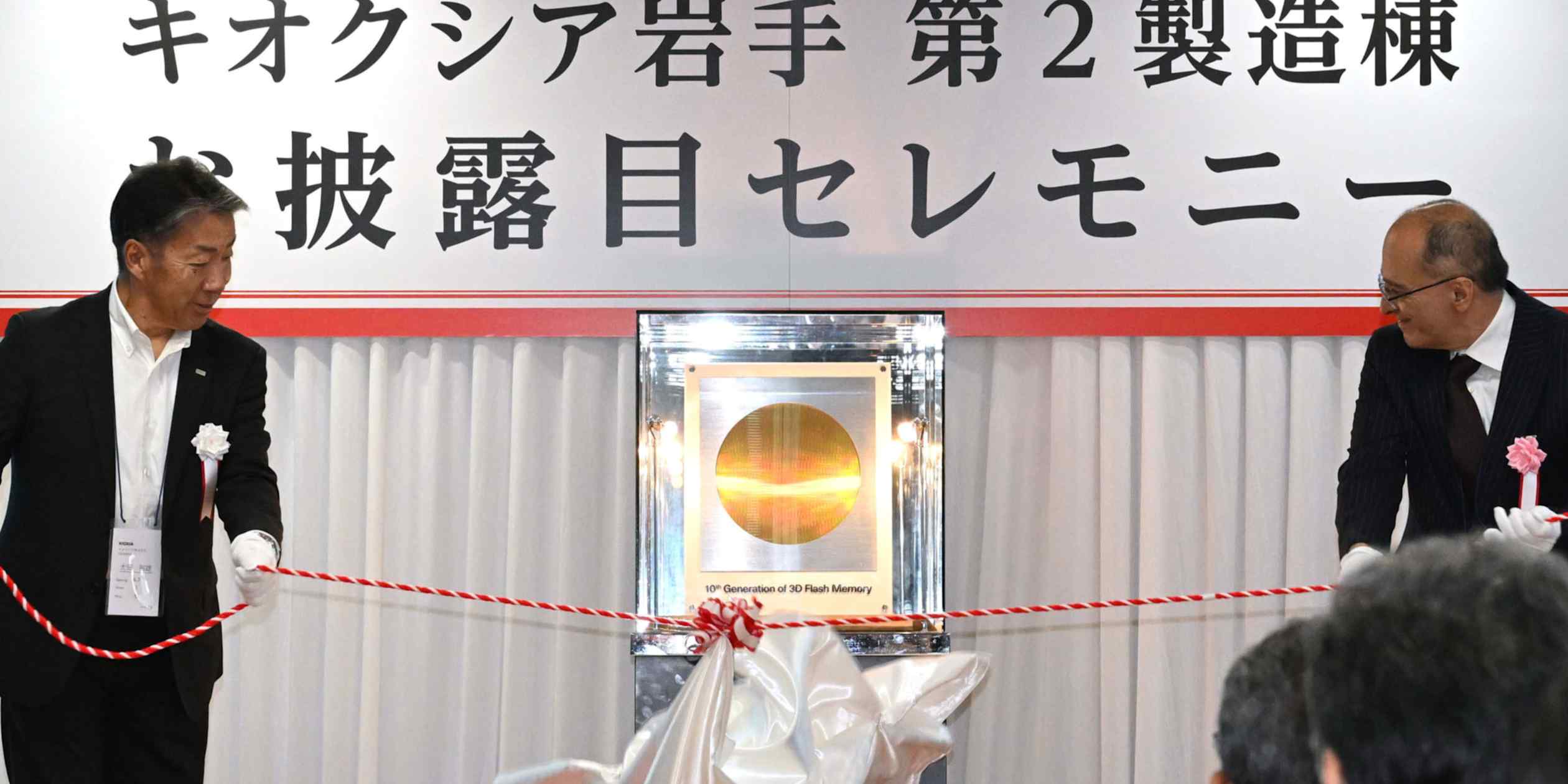
Kioxia Corporation and Sandisk Corporation have officially kicked off production of their 10th-generation 3D Flash memory, known as BiCS Flash, at the Fab2 facility of the Kitakami Plant in Iwate Prefecture, Japan. The production start date: July 3, 2026.
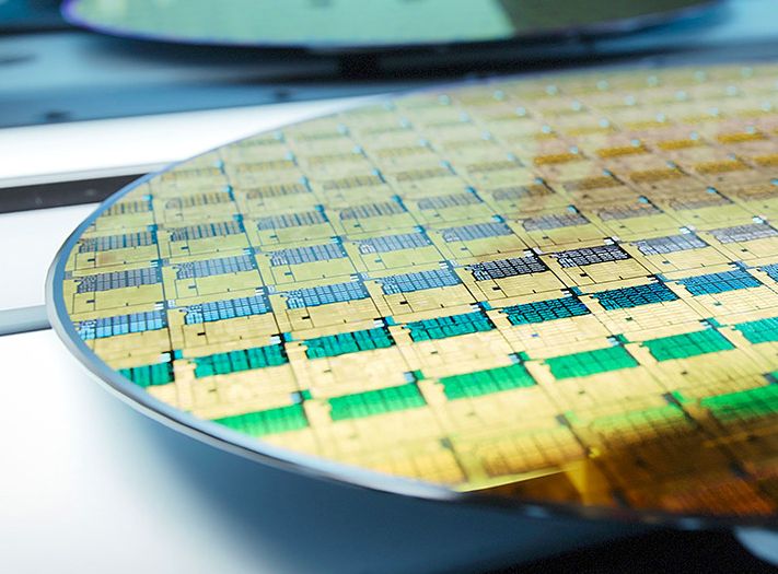
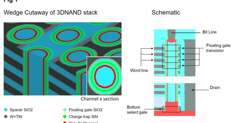
The new generation packs 332 memory layers into a single chip, delivers interface speeds of 4.8 Gb/s (a 33% jump over previous generations), and slashes power consumption meaningfully. Input power drops by 10%, while output power falls by 34% compared to prior generations. The 332-layer design uses CMOS Bonded to Array (CBA) technology, which means the logic circuitry gets bonded directly beneath the memory array rather than sitting beside it. The result is a 59% improvement in bit density.
The Kitakami Plant’s Fab2 facility only opened in September 2025, initially producing 8th-generation chips with 218 memory layers.
Kioxia and Sandisk have also extended their manufacturing joint venture through December 2034, with both companies committing to roughly a 40% year-over-year increase in capital expenditure.
The Kioxia-Sandisk alliance accounts for approximately 28-29% of global flash memory production. The 4.8 Gb/s interface speed reduces the bottleneck between storage and compute. Competitors Samsung, SK Hynix, and Micron are all pursuing their own high-layer-count 3D NAND roadmaps.