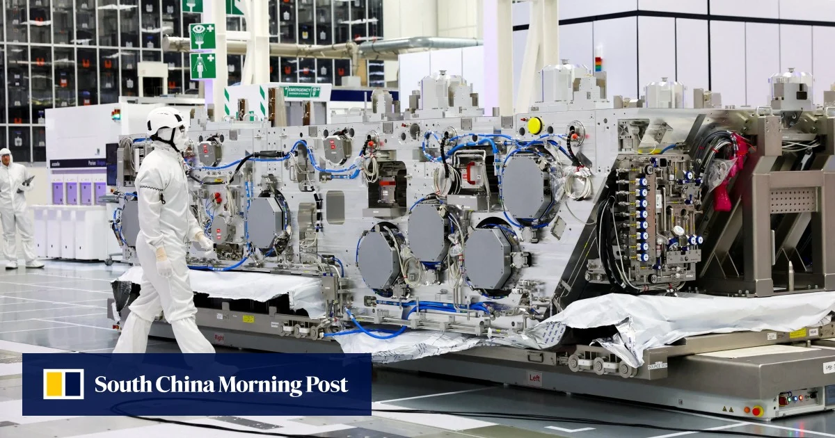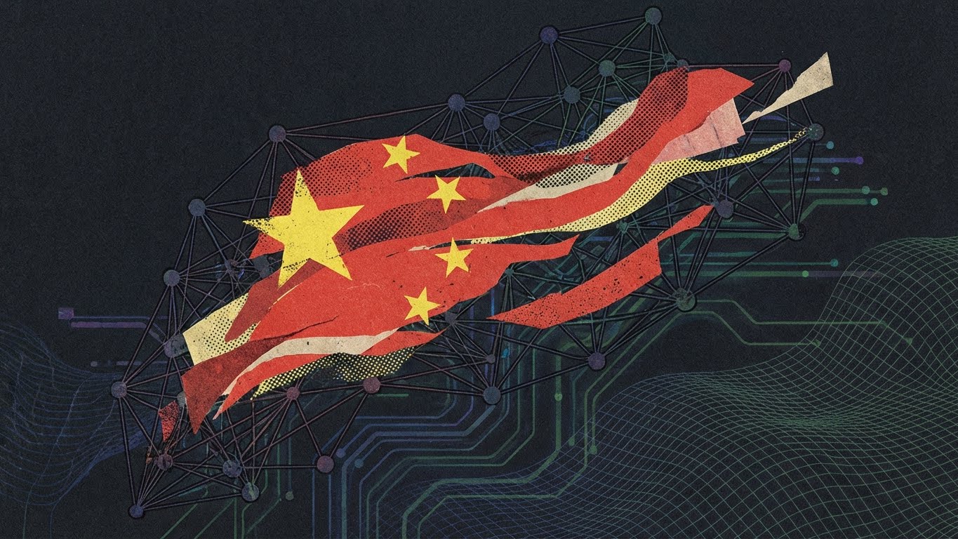
For the past 20 years, advanced semiconductor manufacturing has been dominated by a small set of companies in the Netherlands, Japan, Germany, Taiwan, South Korea, and the United States, largely due to the proprietary technology involved in producing such chips. China, however, has been trying to drain that moat. When Reuters reported in December 2025 that researchers in Shenzhen had secretly built a prototype for an extreme ultraviolet (EUV) lithography machine, an indispensable piece of equipment for producing the most advanced chips, commentators debated when China will be able to overcome one of the last remaining obstacles to manufacturing its own advanced semiconductors.
Whether this prototype is a near-term inflection point or a mere steppingstone on a long journey remains difficult to predict. Chinese insiders claim that 2030 is a “realistic target” for making working chips from its prototype, while skeptics posit that it will take decades to reach commercial viability.
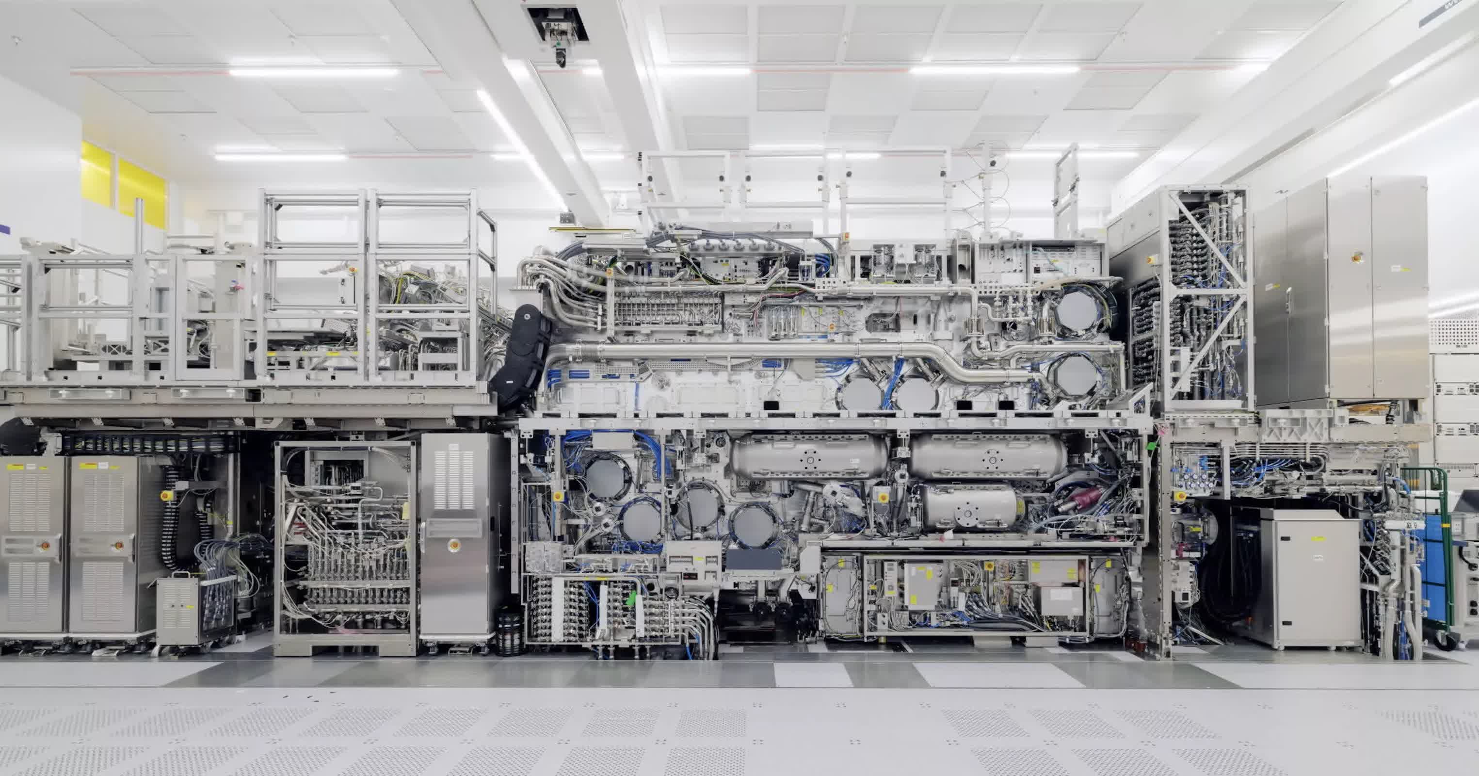
There is a way to cut through the noise. Building an EUV machine depends on specific technical chokepoints that can be identified and monitored. Three of the most important are developing high-power, ultra-low-wavelength light sources that print the circuit patterns; creating incredibly smooth mirrors that reflect EUV light onto silicon wafers with atomic-scale precision; and producing the ultra-pure, light-sensitive photoresist chemicals which convert the light blueprint into a physical stencil for the chip’s microscopic wires.