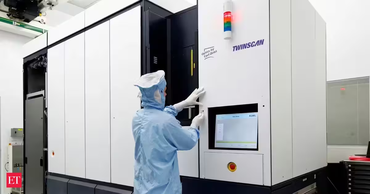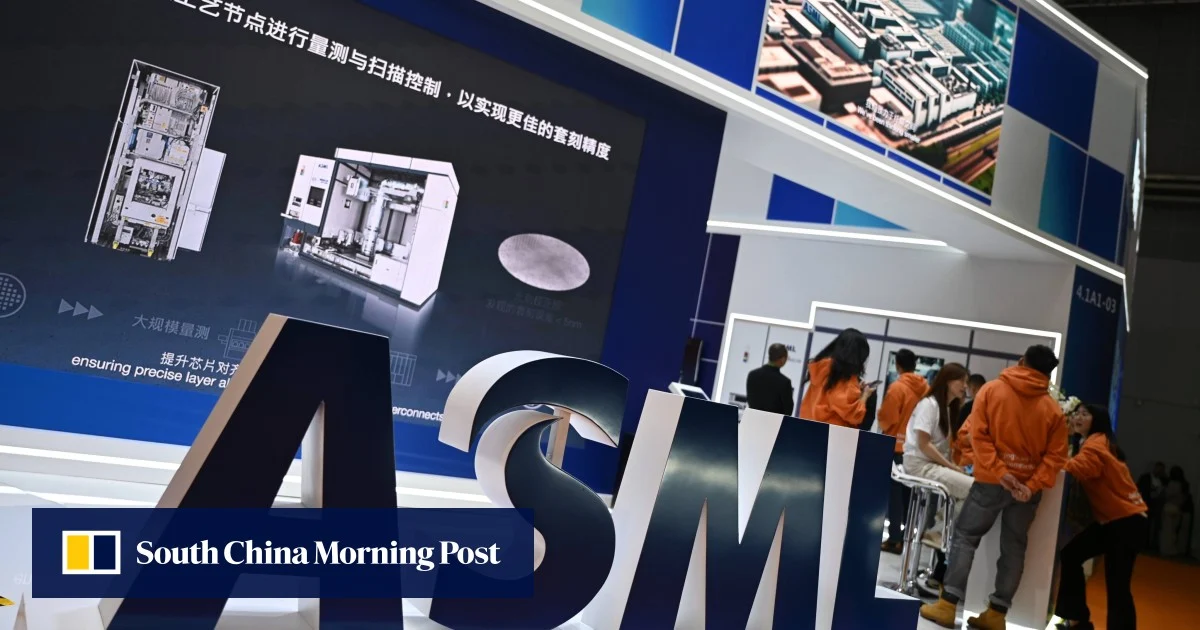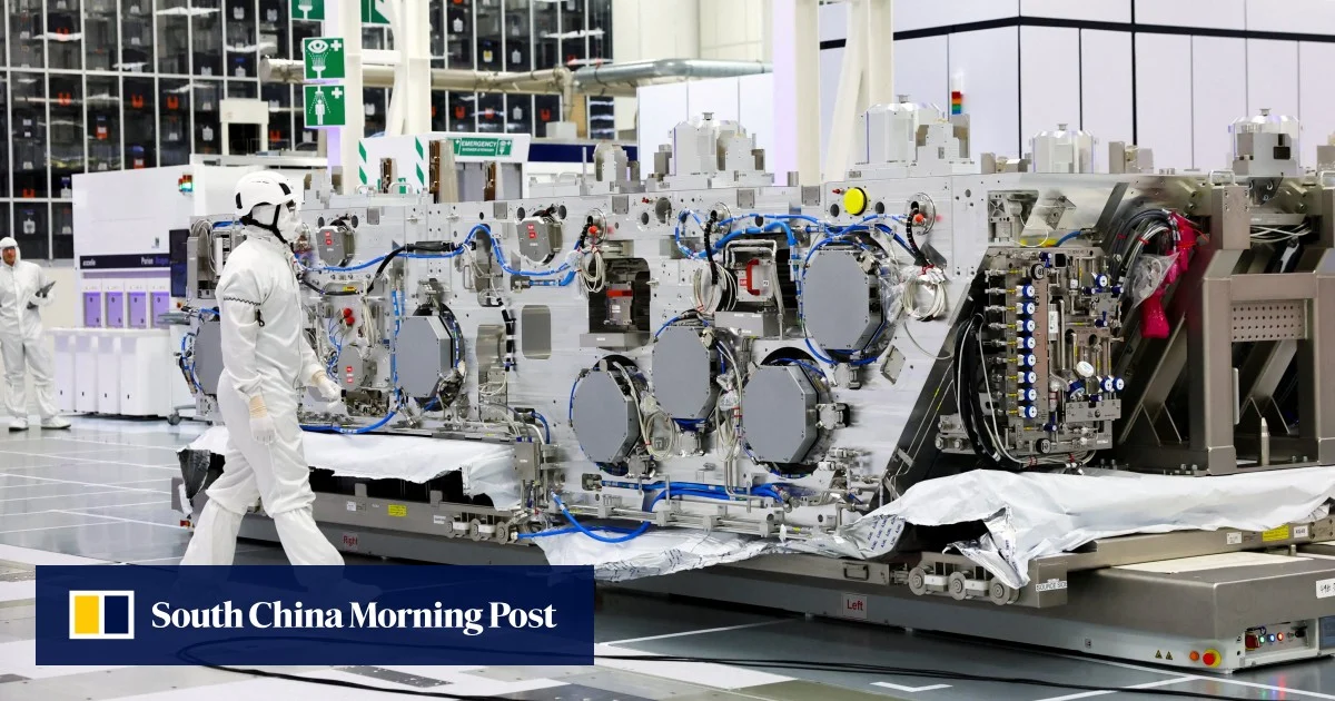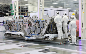
Samsung, SK hynix retain technology lead, but experts warn China’s state-backed drive could narrow the gap A partially assembled ASML EUV machine is seen at the headquarters of Belgian chip research lab IMEC, in Leuven, Belgium (Reuters-Yonap) Recent reports that China has developed its own immersion deep-ultraviolet lithography system have jolted the global semiconductor industry, suggesting that Beijing may be closing one of the most formidable technology gaps maintained by US export controls.Korean experts caution, however, that building the machine is only the first step. China could still need years to prove that the equipment can operate reliably, process wafers at competitive speeds and deliver commercially viable chip yields.Still, Beijing’s steady progress toward semiconductor self-sufficiency should not be underestimated, Korea's Industry Minister Kim Jung-kwan said Thursday. He called the reported advance “shocking and faster than expected."“China is advancing step by step in semiconductors despite the limited profitability of many Chinese chipmakers backed by massive state support,” Kim said.The lithography hurdleImmersion DUV is a mature technology used for years by leading chipmakers, primarily through systems supplied by Dutch equipment giant ASML. It projects light through a thin layer of water to print finer circuit patterns than conventional dry DUV systems. More advanced chip production increasingly relies on ASML’s extreme-ultraviolet and high-numerical-aperture EUV equipment.Blocked from buying advanced lithography systems, Chinese chipmakers have relied largely on older dry DUV equipment from ASML. Those machines are said to trail its newest models by about eight generations and are used mainly to produce legacy chips on 20- to 28-nanometer processes.Chinese companies have reportedly pushed older equipment to produce 7-nanometer-class chips through multipatterning, though their yields and production economics remain unclear.A domestically developed immersion DUV system could help China move toward smaller process nodes. But determining whether the equipment is suitable for stable mass production could take at least two to three years, according to Shim Dae-yong, an electrical engineering professor at Dong-A University and former SK hynix vice president specializing in high-bandwidth memory.“Lithography is widely considered the most difficult of the roughly 800 steps involved in chipmaking, which also include deposition, etching and cleaning,” Shim said.“Having the machine does not mean the work is finished. Even SK hynix needed two to three years to tune its processes and achieve meaningful yields after adopting ASML’s ArF immersion DUV equipment.”The difficulty grew as chipmakers moved below 30 nanometers. At those dimensions, DUV requires multipatterning, which divides a circuit pattern across several exposures that must be aligned with extreme precision through additional processing steps.The method allowed the industry to manufacture 14-nanometer, 10-nanometer and even 7-nanometer-class chips before EUV entered mass production. But the added steps increased complexity, costs and the risk of defects.“Scaling with DUV was extremely difficult, and once we reached its limits, we shifted to EUV,” Shim said. SK hynix faced a similar learning curve after adopting EUV and expanded its use gradually as it stabilized the technology, he added.China’s system may eventually be capable of producing advanced chips, but initial yields could remain at 10 to 20 percent, Shim said. Mass production generally requires yields of at least 70 percent, while profitable production often demands levels closer to 90 percent.Throughput and yields remain criticalKim Hyung-jun, an emeritus professor at Seoul National University and head of the state-led Next Generation Intelligence Semiconductor Foundation, offered a similar assessment.China’s newly developed machine is understood to be an early single-stage system, compared with the dual-stage architecture used in ASML equipment. Dual-stage systems can measure and align one wafer while another is being exposed, improving productivity.“What matters is throughput — how quickly the equipment can process wafers,” Kim said. “Given that it is a single-stage tool, it will take considerable time before China can produce meaningful results.”Using older or less efficient equipment to manufacture advanced chips requires more processing steps, increasing production time and the cost of each usable chip.China, however, may be able to absorb those disadvantages through state funding, government procurement and policies encouraging electronics manufacturers to use domestically produced semiconductors.“They may lack the yields, and producing one advanced chip with older tools can become extremely expensive,” Kim said. “But if the government requires electronics manufacturers to use domestic chips and creates a funding cycle around the industry, companies can continue building scale.”Lithography equipment also cannot simply be installed and operated as a stand-alone tool. Chipmakers typically spend years working with equipment suppliers such as ASML, Tokyo Electron and Applied Materials to fine-tune process conditions, integrate production stages and stabilize yields.China would therefore need to develop not only the lithography machine but also the surrounding ecosystem of materials, components, software, maintenance and process expertise.Korean chipmakers push aheadAs China works to establish an independent semiconductor supply chain, Samsung Electronics and SK hynix are already moving toward the next generation of memory technology.ChangXin Memory Technologies’ DDR5 chips, reportedly manufactured using a fourth-generation 1a DRAM process, and its HBM3 products are considered comparable to technologies introduced by Korean memory makers several years ago.Samsung is expanding HBM4 sales while developing HBM4E and zHBM, a three-dimensional architecture that stacks high-bandwidth memory directly above an AI processor to shorten data-transfer distances.SK hynix is developing hybrid bonding, HBM5 and iHBM, which are intended to improve integration and address the mounting heat challenges of next-generation AI memory.China’s reported lithography advance may therefore pose little immediate threat to Korean chipmakers. But experts said its willingness to tolerate low profits and high costs while building domestic capabilities could steadily narrow the technology gap.
China’s homegrown DUV jolts chip industry, but yield test looms
Recent reports that China has developed its own immersion deep-ultraviolet lithography system have jolted the global semiconductor industry, suggesting that Bei
906 words~4 min read