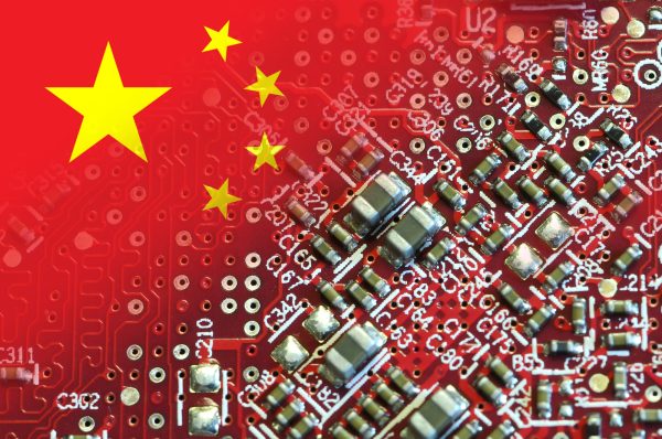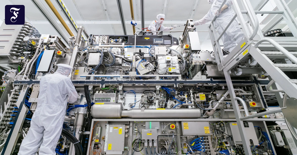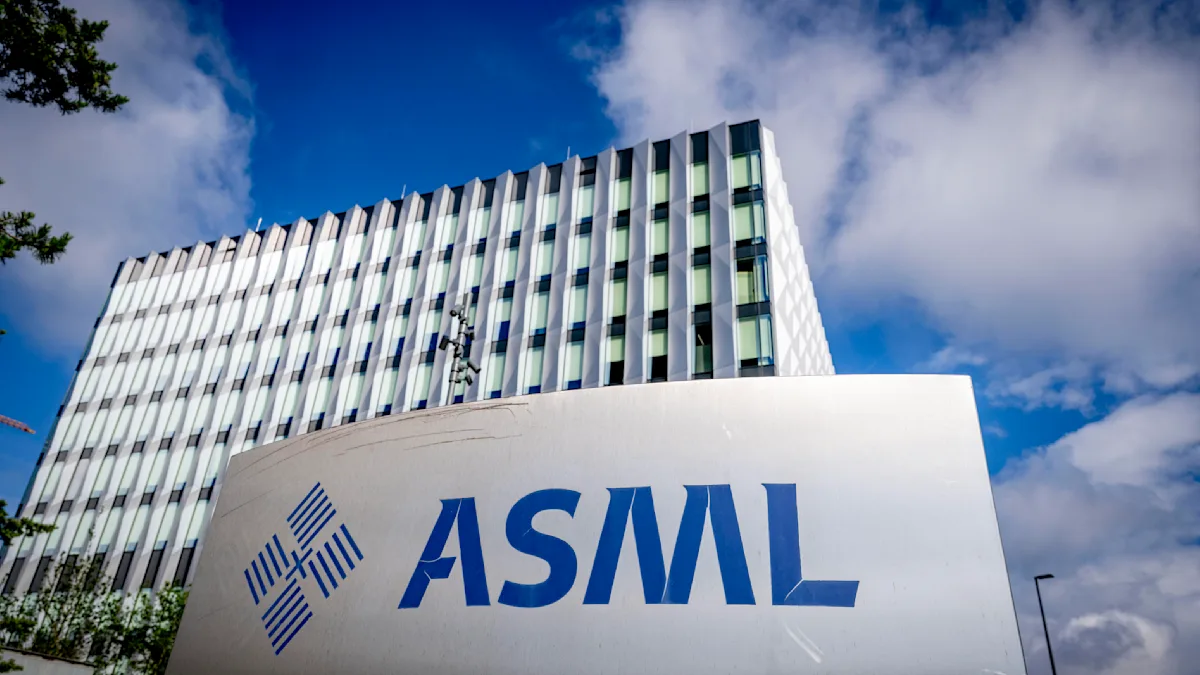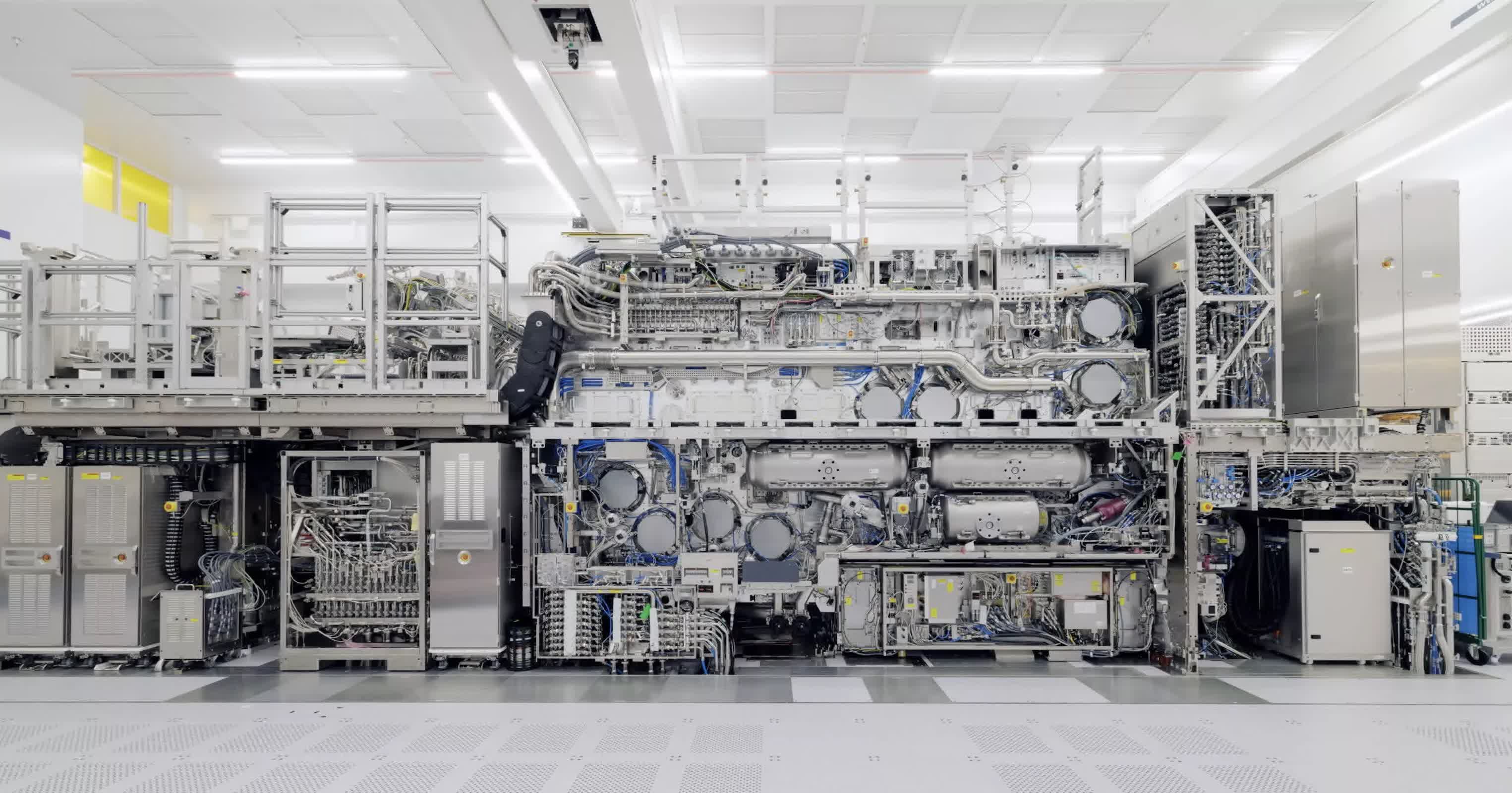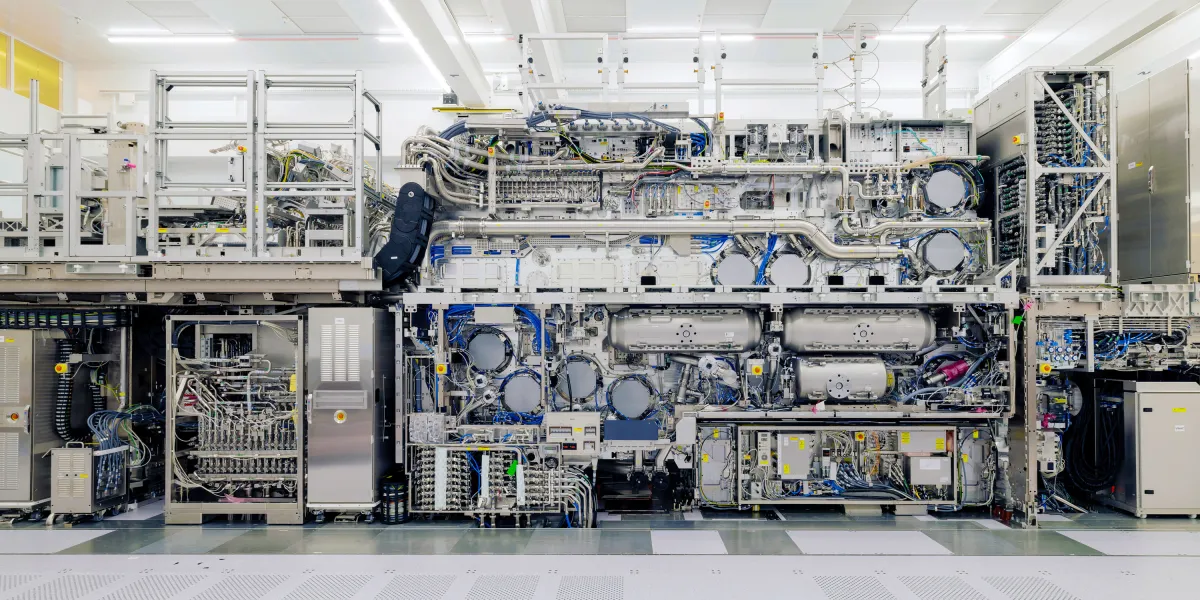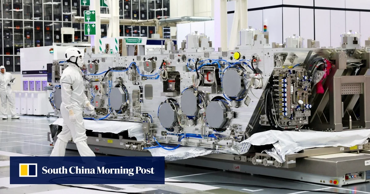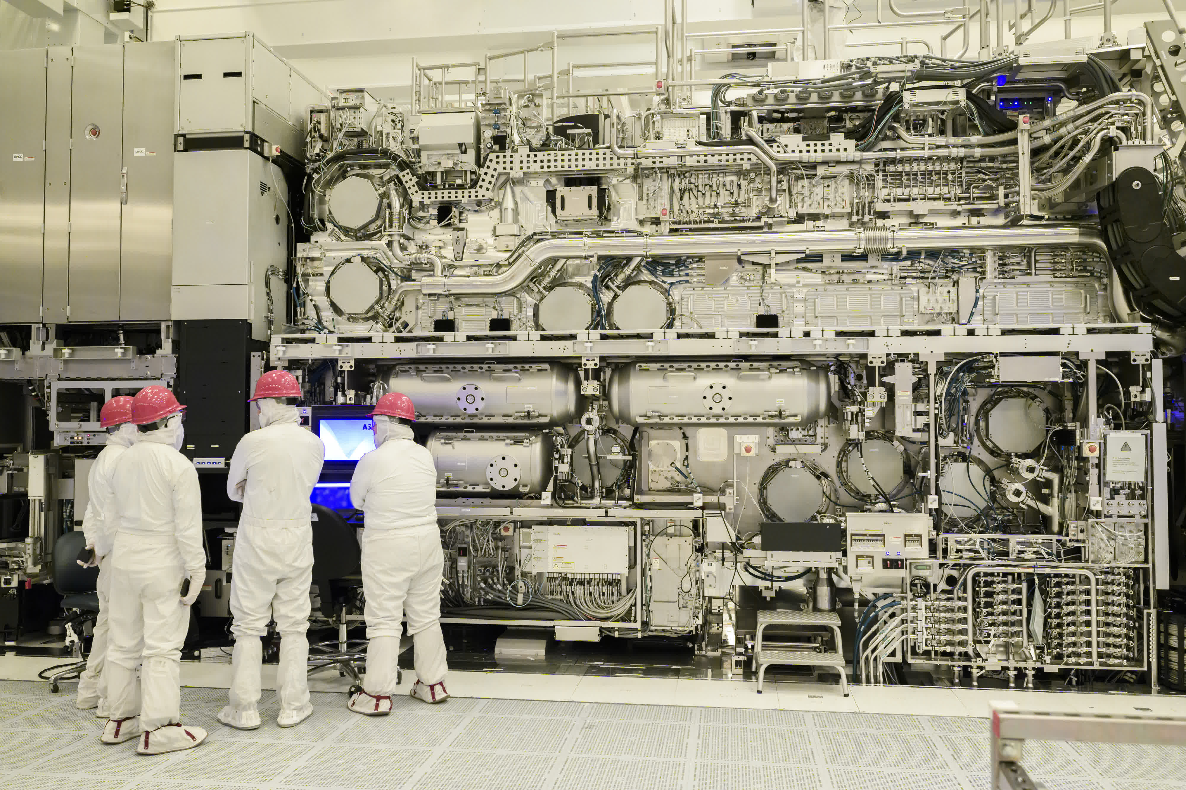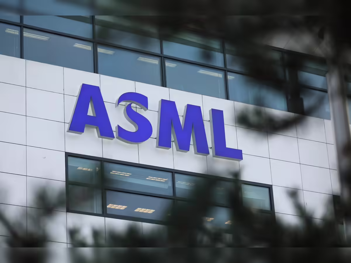
Every advanced processor on the planet passes through the same bottleneck. The chip inside the newest iPhone, the silicon training the world's largest AI models, the processors steering a modern fighter jet — each one is printed by a machine that a single company knows how to build. That company sits in Veldhoven, a Dutch town most people could never place on a map. Its name is ASML, and its hold on the most advanced chipmaking tool ever made comes close to total.A stealth startup in San Francisco believes it has found another way in. Rather than the door ASML guards, it wants to open a different one — a door lit by X-rays.The startup is called Substrate. It carries the ambition, the money, and the founder charisma that Silicon Valley reserves for its longest shots. It also carries a history that should make any semiconductor engineer pause, because the road Substrate wants to walk is lined with the wreckage of companies and laboratories that tried the same thing and turned back. The question worth answering is a plain one, stripped of the hype that surrounds a well-funded launch. Does Substrate have a real shot at breaking the most valuable monopoly in technology, or is this the most expensive physics experiment of the decade?Key TakeawaysSubstrate is a stealth US startup pitching X-ray lithography as an alternative to ASML's extreme ultraviolet (EUV) machines, the tools behind every cutting-edge chip.Its founder, James Proud, is a former Thiel Fellow best known for the failed sleep-tracking company Hello, maker of the Sense device.ASML holds a complete monopoly on EUV lithography. Its newest High-NA machines carry a price tag around 350 to 400 million dollars each, a figure worth verifying against current pricing.X-ray lithography is an old idea. IBM and others pursued it through the 1980s and 1990s, then walked away once the surrounding technology proved too hard to assemble.The physics of a shorter wavelength is genuinely attractive. The engineering ecosystem around it — masks, resists, fab integration — remains the graveyard where past attempts died.For India's chip ambitions, a cheaper and simpler advanced-lithography tool would matter enormously. For now it stays a promise on a slide.What is Substrate, and who is James Proud?Substrate emerged from stealth in late 2025, according to reporting around its launch, with a funding round said to sit near 100 million dollars and a valuation reported at over a billion. Those figures deserve a careful second look against primary sources, because a stealth launch is precisely the moment when a company controls its own story. The named backers reported at the time included marquee venture names and, tellingly, capital linked to the US intelligence and defence community. If that last detail holds, it tells you as much about the company's ambitions as any technical white paper could, because it points at Washington rather than at Wall Street.The founder is James Proud, a British entrepreneur who arrived in Silicon Valley young and left school for a Thiel Fellowship, the programme that pays bright people to skip university and build. His previous act was Hello, a startup that made the Sense sleep tracker, a glowing orb for the bedside table that promised to read your nights and improve them. Hello raised heavily, sold well on early enthusiasm, and then collapsed around 2017 when the hardware economics refused to cooperate. Proud carries that arc into Substrate, and it cuts both ways. The bull reading is that he has learned the brutal lessons of hardware at scale. The bear reading is that a consumer gadget that flopped is a strange launchpad for the most demanding manufacturing tool humanity has ever attempted.Substrate's stated mission reaches past any single product. The company talks about rebuilding advanced chip manufacturing inside the United States, about breaking a dependence on foreign tools, about a domestic path to the frontier of computing. That is a national-security pitch dressed in startup clothing, and it lands at a moment when Washington is spending heavily to bring chipmaking home.Why does one Dutch company control the world's most advanced chips?To understand what Substrate is attacking, you have to understand what ASML built, and why nobody else has matched it.Making a modern chip means printing patterns onto silicon at sizes far smaller than a virus. The tool that does the printing is a lithography machine, and the finest patterns today are printed using extreme ultraviolet light with a wavelength of 13.5 nanometres. Generating that light is closer to sorcery than to plumbing. Inside an ASML EUV machine, droplets of molten tin fall through a vacuum and are struck twice by a high-power laser, vaporising into a plasma that glows at exactly the right wavelength. That light bounces off a series of mirrors so smooth that, scaled to the size of a country, their largest bump would measure a fraction of a millimetre. The whole apparatus fills a room and weighs as much as a couple of buses.ASML is the only company on Earth that can make this machine work at production scale. It took the firm decades and tens of billions in research, drawing on a supply chain that stretches from a German optics maker to an American laser company ASML later bought outright. The result is a monopoly with few equals in industrial history. TSMC, Intel, and Samsung all queue for the same tool from the same vendor. The newest version, called High-NA EUV, pushes resolution further and carries a price reported around 350 to 400 million dollars per system, a number worth checking against the latest disclosures.Two facts follow from this, and both matter for Substrate. First, whoever controls advanced lithography controls the pace of computing itself, which is why the machines are barred from sale to China and sit at the centre of a trade war. Second, a monopoly this deep invites challengers, because the prize for cracking it would be measured in hundreds of billions. Substrate has walked toward that prize. So have others, and the walking is the easy part.How does chip lithography actually work?Strip away the physics and lithography is printing. That comparison is more than a convenience, because photolithography descends from the same family as the printing press, and the same logic governs both. You have a pattern you want to reproduce, a stencil that holds it, a light or an ink that transfers it, and a surface that receives it. Gutenberg pressed inked metal type onto paper. A chip fab presses patterned light onto a silicon wafer coated with a light-sensitive chemical called a resist. Where the light lands, the resist changes, and the pattern is fixed into the material below.The difference is one of scale that beggars the imagination. Gutenberg's type measured a few millimetres. The features a modern fab prints measure a handful of nanometres, tens of thousands of times finer than the width of a human hair. To reach that fineness, the industry has spent sixty years shrinking the wavelength of the light doing the printing, because a coarser light cannot draw a finer line, the way a fat marker cannot letter a postage stamp. Visible light gave way to ultraviolet, ultraviolet gave way to deep ultraviolet, and deep ultraviolet finally gave way to the extreme ultraviolet that ASML alone can deliver.Each shrink in wavelength demanded a new kind of press. EUV light refuses to pass through ordinary lenses, so ASML had to abandon lenses altogether and print by reflection off mirrors. Every step down the wavelength ladder rebuilt the print shop from the floor up, and every rebuild took a decade and a fortune. That is the pattern Substrate is trying to break, and it wants to break it by jumping the queue — skipping past EUV to a light so short that, on paper, it makes today's finest print run look coarse.What is X-ray lithography, and why does Substrate think it wins?Here is the elegant core of the pitch. X-rays sit far down the wavelength ladder from extreme ultraviolet. Where EUV works at 13.5 nanometres, the soft X-rays relevant to lithography measure around one nanometre or below. A shorter wavelength can, in principle, draw a finer and sharper line, and it can do so with a physics that sidesteps some of the maddening limits EUV runs into as features shrink. That is the seed of truth at the heart of Substrate's argument, and it is a real one. Lithographers have understood for decades that shorter is sharper.Substrate's reported approach uses a particle accelerator as its light source rather than the tin-droplet plasma ASML relies on. An accelerator can produce X-rays with a brightness and stability that older X-ray schemes lacked, and the company argues this changes the economics that sank earlier efforts. The pitch, as reported, extends to bold performance claims — the ability to print features around 12 nanometres, and a cost per wafer that could fall dramatically toward the end of the decade, with figures such as 10,000 dollars a wafer and target dates around 2030 circulating in coverage of the launch. Treat every one of those numbers as a claim rather than a result, because as of now they describe a destination, not an arrival.The company's real argument is about cost and control as much as resolution. If an accelerator-based X-ray tool could be built more simply than an EUV machine, and manufactured domestically, it would attack ASML at its two strongest points at once — the price and the geography. That is the theory. Below is how that theory lines up against the incumbent, with the crucial caveat that one column is proven and the other is promised.AttributeASML EUV (proven)Substrate X-ray (claimed)Wavelength13.5 nanometresaround 1 nanometre or belowLight sourceLaser-pulsed tin plasmaParticle acceleratorMachine cost~150m to 400m dollars (verify)Claimed to be far lowerMaturityIn high-volume production worldwidePre-production, no shipping toolAvailabilityASML onlySubstrate only, developmentalEcosystemMature masks, resists, fabsLargely unbuiltThe table flatters neither side unfairly. It simply shows that Substrate competes on paper against a tool that competes in factories.Why did the chip industry abandon X-rays before?This is where the story climbs into thinner air, and where the honest reporting lives.X-ray lithography is old. Through the 1980s and 1990s, IBM poured serious resources into it, building synchrotron light sources and betting that X-rays would carry chipmaking into the future. Japanese electronics giants ran their own programmes. For a stretch, X-ray lithography looked like the summit the whole industry would climb toward. Then, one by one, the expeditions turned back. The approach stalled, the money moved to deep ultraviolet and later to EUV, and X-ray lithography became a cautionary tale told to young engineers.The reasons it stalled are the reasons to keep a cool head about Substrate now. The problem was rarely the light itself. The problem was everything around the light. A lithography tool is only the base camp of a far larger ascent. You need photomasks that can hold a pattern at X-ray wavelengths, and X-rays are so penetrating that making a mask which blocks them cleanly is punishing. You need resists tuned to the new light. You need an entire fab willing to rebuild its process around an unproven tool, and a fab is a 20-billion-dollar bet that few will stake on a newcomer. Past X-ray efforts reached a certain altitude and found the air too thin to go further. Their frozen attempts still mark the route, and any climber setting out today passes them on the way up.Substrate's counter is that the mountain has changed. Accelerator technology has matured. Manufacturing has advanced. The tools to build the surrounding ecosystem exist now in ways they did not thirty years ago. That counter is reasonable, and it is also exactly what every well-funded attempt on a deadly summit says at base camp. Whether the conditions have genuinely shifted, or whether Substrate has simply arrived with better equipment at the same lethal altitude, is the question that will decide the company, and it will take years and demonstrated hardware to answer.Can Substrate really challenge ASML?The fair answer holds two truths at once, and refusing to collapse them into a single verdict is the whole discipline of covering a story like this.The bull case has teeth. The physics of a shorter wavelength is sound. A domestic, cheaper alternative to ASML would find eager buyers among governments desperate to secure their own chip supply. The founder has raised real money from serious backers who have seen the pitch in full, which counts for something even when it settles nothing. And monopolies do fall, sometimes to challengers everyone had written off. ASML itself was once the underdog, dismissed for years before EUV came good.The bear case has more teeth. A light source is the beginning of the problem, rather than the end of it. ASML's monopoly rests less on its ability to make EUV light and more on the thirty-year ecosystem it assembled around that light — the mask makers, the resist chemists, the metrology firms, the fabs that rebuilt themselves around the tool. Substrate would have to conjure that entire supporting cast from scratch, and persuade a chipmaker to bet a fab on it. Semiconductor history is unkind to elegant physics that lacks an ecosystem. The graveyard has a name for it, and that name is X-ray lithography.There is also the founder's own record to weigh with clear eyes. A sleep-tracker that failed is a thin foundation for the hardest tool in manufacturing, and confidence is the one raw material Silicon Valley never runs short of. None of this makes Substrate a fraud. It makes Substrate a moonshot, and moonshots deserve to be reported as moonshots rather than as done deals.Why is the US government interested in a chip startup?Follow the reported money and the strategy comes into focus. If capital tied to the US defence and intelligence community sits on Substrate's cap table, the company is more than a commercial bet. It is a hedge.Washington has watched with unease as the entire frontier of computing came to depend on a single Dutch supplier and a single Taiwanese manufacturer sitting a short missile flight from the Chinese mainland. The US CHIPS Act poured tens of billions into bringing chip manufacturing back onto American soil, yet even a fab built in Arizona still fills its cleanrooms with ASML machines shipped from the Netherlands. A domestic lithography tool would close that last gap in the chain, turning chip independence from a slogan into something closer to fact.That strategic hunger explains why a pre-production startup could raise at a billion-dollar valuation on physics that remains unproven. The government is buying an option, not a product. If Substrate works, the payoff is sovereignty over the most strategic technology on Earth. If it fails, the cost is a rounding error against a defence budget. Seen that way, the bet becomes rational even at long odds, which is a useful thing for readers to grasp, because it explains money that otherwise looks reckless.What does Substrate mean for India?For Indian readers, the interest is direct rather than academic, and it turns on a single word — cost.India has staked real ambition on the India Semiconductor Mission, and the money has begun to move. Tata is building the country's first major fab at Dholera in Gujarat in partnership with Taiwan's Powerchip, and Micron has an assembly and test plant running near Sanand. Yet every one of these facilities aims at mature, trailing-edge chips, the workhorses that run cars and appliances, rather than the leading-edge processors that ASML's machines produce. The reason is partly cost and partly access. A single High-NA EUV tool costs more than the equipment budget of an entire mid-sized fab, and the queue for ASML's output is long, with priority going to customers who have bought from the firm for decades.This is the gap where a cheaper alternative would matter to a latecomer nation. A lithography tool that cost a fraction of ASML's price, and that a new entrant could actually buy, would lower the wall that keeps countries like India away from the leading edge. It would let a national programme aim higher than trailing-edge chips without first spending a decade earning a place in ASML's order book. That is the prize Substrate dangles for every aspiring chip nation, India included.The word to hold onto is would. As things stand, Substrate has a pitch, a founder, reported funding, and a physics argument. India's fabs will run on the tools that exist and ship, which today means ASML and its established rivals. A cheaper X-ray future stays worth watching precisely because the stakes for a country trying to climb the ladder late are so high. The tool that reaches production first, at a price a newcomer can pay, reshapes who gets to sit at the frontier — and that is a contest with more riding on it than the fortunes of one San Francisco startup.Frequently Asked QuestionsWhat is Substrate?Substrate is a US startup, reported to have emerged from stealth in late 2025, that is developing X-ray lithography as an alternative to the EUV machines ASML sells for making advanced chips. It was founded by James Proud.Who is James Proud?James Proud is a British entrepreneur and former Thiel Fellow. He earlier founded Hello, the company behind the Sense sleep tracker, which shut down around 2017. Substrate is his return to hardware, aimed at a far harder problem.How is X-ray lithography different from ASML's EUV?ASML's EUV machines print chip patterns using light at a 13.5-nanometre wavelength, generated by vaporising tin with a laser. X-ray lithography uses a far shorter wavelength, around one nanometre or below, which in theory can draw finer lines. Substrate reportedly generates its X-rays with a particle accelerator.Why did X-ray lithography fail before?IBM and others pursued it in the 1980s and 1990s, then abandoned it. The light itself worked. The surrounding ecosystem — masks that could block X-rays cleanly, matched resists, and fabs willing to rebuild around an unproven tool — proved too hard and too costly to assemble at the time.Is Substrate a real threat to ASML?As of now it is an early-stage moonshot rather than a shipping competitor. The physics is credible, the funding is reportedly real, and the strategic interest from Washington is understandable. Yet ASML's strength lies in a thirty-year ecosystem that Substrate would have to rebuild from scratch, and no chipmaker has committed a fab to the approach.What would it mean for India?A cheaper and more accessible advanced-lithography tool would lower the barrier that keeps latecomer nations, India among them, away from leading-edge chipmaking. For now India's fabs at Dholera and Sanand target mature chips using established tools, so the relevance stays forward-looking rather than immediate.end of article
Substrate Bets X-Ray Lithography Can Outdo ASML's EUV Chip Machines
One Dutch company controls the machine behind every leading-edge processor on Earth. Substrate wants to route around it using X-rays instead of extreme ultraviolet light. Here is what stands up, what remains a pitch, and why chipmakers from Taiwan to Dholera are watching.
3,102 words~14 min read