Skip to content
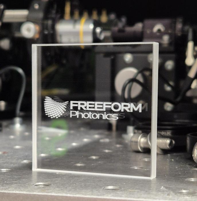
Glass-based substrates are slowly beginning to push out organic substrates commonly used in PCBs due to often superior material properties. One area where glass substrates have however struggled is with through-hole vias and providing the conductive copper path through them. A 2024 article by [Keith Best] gives a good overview of the topic, with recent news showing how much companies like Intel are pushing for glass substrates, specifically for the packaging of dies.
One major advantage with vias in glass substrates is that they can be much smaller, enabling smaller than 0.1 mm diameter holes with far finer pitch. The challenge here is to make perfect holes with a laser that are defect-free, as well as have the intended diameter.
After that this through-glass via (TGV) has to be coated or filled with copper, much like their organic equivalent. Said TGV can be fully filled with copper, or use plating and add dielectric filler. Detecting flaws in such a finished TGV is important.
In a 2025 review article of glass substrate technologies by [Pratik Nimbalkar] et al. published in Chips the state of the art at the time was covered. The need for ever higher-density integration options with ASICs is highlight here, especially now that many chips today consist of multiple interconnected dies inside a single package.