HomeAI · summaries
Storia in 2 fonti
Nvidia may redesign Feynman AI platform due to manufacturing constraints
Nvidia's Feynman GPU architecture targets 2028 deployment on TSMC's 1.6 nm A16 process with 3D die-stacking and custom high-bandwidth memory for
Confronto fonti
2 prospettive sulla stessa storiaTimeline cronologica
- ·
benzinga.com
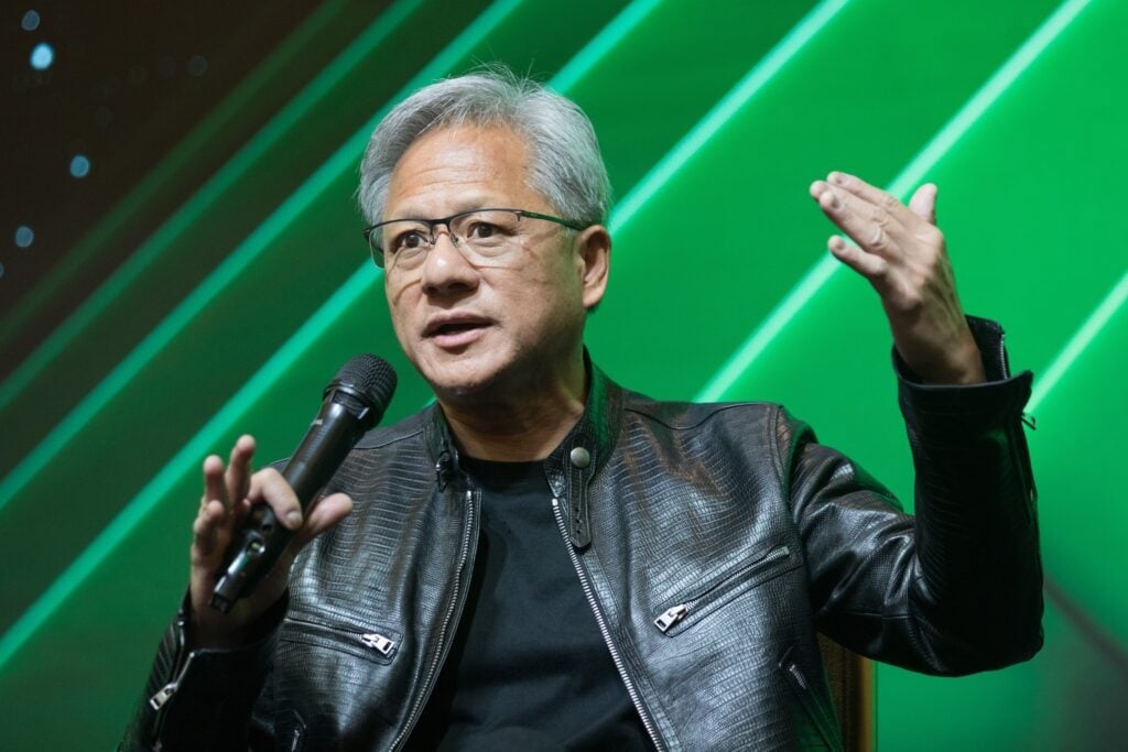
Nvidia's Next-Gen Feynman AI Platform Is Ramping Up, Forcing TSMC to Race Ahead: Report - NVIDIA (NASDAQ:
Nvidia is reportedly accelerating Feynman development, pushing TSMC to ramp 2nm and advanced packaging capacity.
- ·
cryptobriefing.com
Nvidia may redesign Feynman AI platform due to manufacturing constraints
Nvidia's Feynman GPU architecture targets 2028 deployment on TSMC's 1.6 nm A16 process with 3D die-stacking and custom high-bandwidth memory for