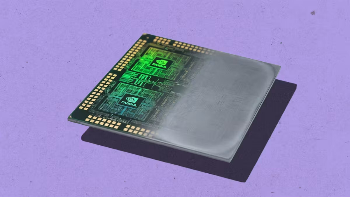
Nvidia is pushing forward with its Feynman GPU microarchitecture, targeting a 2028 release. The platform will be built on TSMC’s A16 process node, measuring just 1.6 nanometers, and will pack in technologies like 3D die-stacking, backside power delivery, and custom high-bandwidth memory.
What Feynman brings to the table
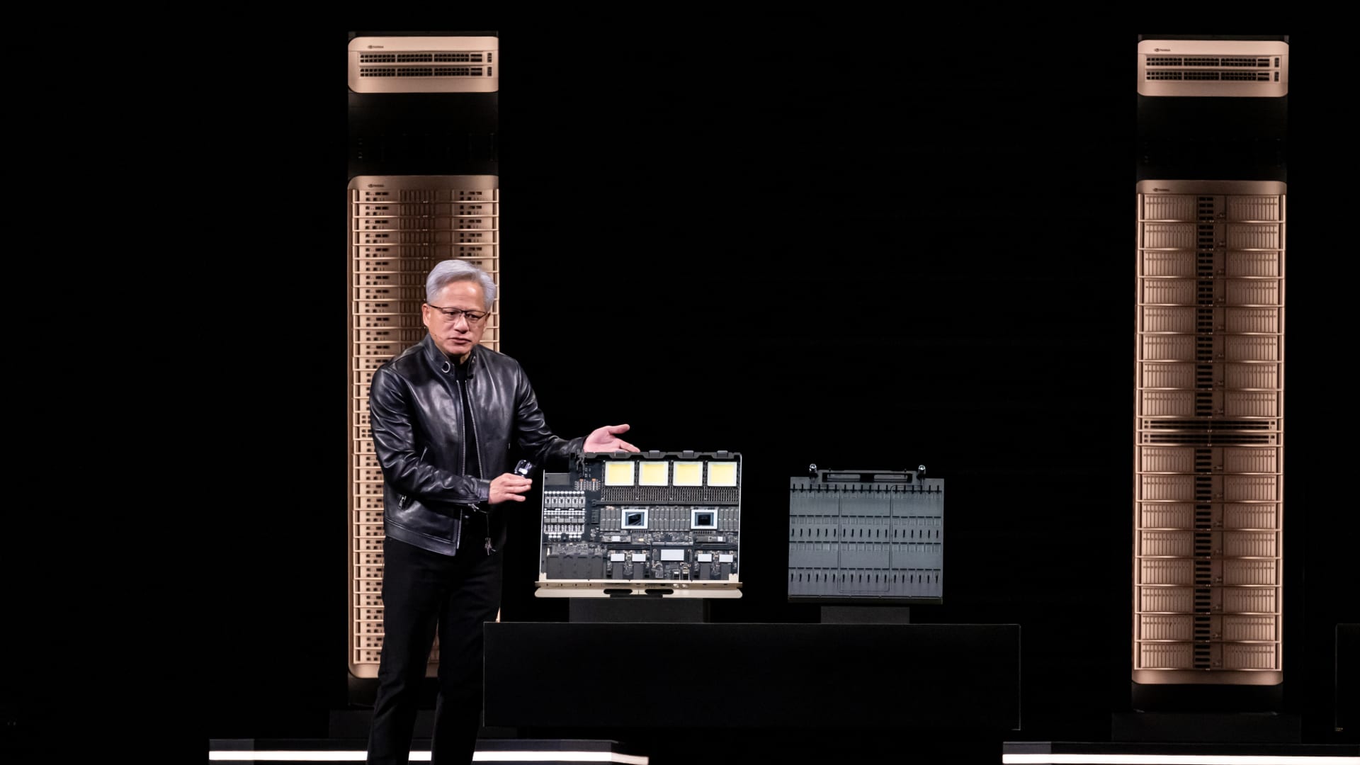
CEO Jensen Huang first unveiled the Feynman architecture at GTC 2025, with additional technical details shared at GTC 2026 in March. Named after legendary physicist Richard Feynman, the platform is designed to succeed the Rubin architecture in Nvidia’s roadmap and will pair with a new CPU called Rosa, which follows the current Vera architecture.
Backside power delivery moves power delivery to the back of the chip, freeing up space for data pathways and improving both performance and energy efficiency.
The TSMC bottleneck