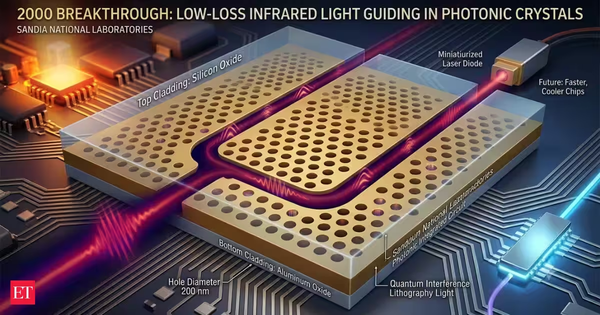
In 2000, researchers at the Department of Energy's Sandia National Laboratories demonstrated a tiny structure that could bend infrared light with very little loss. Made from gallium arsenide, the structure looked more like cheesecloth than an optical device. Its carefully arranged holes allowed selected wavelengths of light to travel through the material while blocking others.The work, published in Nature and Optics Letters, focused on a two-dimensional photonic crystal, an artificial structure designed to conduct light.Researchers said the approach could eventually reduce the energy needed to start and operate lasers. It also offered the potential to replace electronic chips with faster, cooler photonic chips.A tiny crystal built to guide infrared lightThe Sandia structure was made from gallium arsenide without metallic components. It contained a regular pattern of holes whose size and spacing determined which wavelengths could pass through the crystal. The cell centers were spaced 416 nanometers apart, while the holes measured only 200 nanometers across.Electron beam lithography was used to create the openings.The structure could essentially act as a wire for light. Unlike natural crystals, where molecular spacing determines which wavelengths can pass, researchers can vary the spacing of components in an artificial crystal to control the wavelengths it transmits.In laboratory experiments, the Sandia crystal guided infrared light around sharp corners with little measurable intrinsic loss or distortion.Keeping the light inside was the main challengeSandia researchers had previously created three-dimensional silicon photonic crystals that could bend light with little loss. The two-dimensional design was cheaper and easier to build, but it created another problem. Because the structure was essentially two-dimensional, researchers thought light could escape through its top and bottom.They addressed this by placing silicon oxide on top and aluminum oxide underneath the gallium arsenide. The cladding created a large difference in refractive index that dramatically improved the ability to keep light within the central portion of the crystal.The cladding technique had been developed at Sandia as part of its work on vertical cavity stimulated emission lasers, or VCSELs.The nanoscale holes helped confine the lightThe air-filled holes might appear to provide a route for the light to escape. Air has a lower refractive index than the semiconductor, but the openings were so small that quantum interference effects came into play. As a result, the light moved to the next confined substructure rather than simply escaping through the holes.Scientists at MIT calculated the dimensions of the structure, while Sandia researchers Shawn Lin and Edmond Chow led the project.Lin pointed out that the crystal itself was easy to make; the difficult part was building the structure without cracking it and then testing it, as per the Sciencedaily report.The design could bring lasers and light guides togetherThe researchers saw several possible uses for the technology. Much of the energy input to lasers is used to compensate for light that is dispersed during the lasing process. Because the photonic crystal could guide infrared light with very little loss, the technique offered the potential to reduce the energy needed to start and operate a laser.The structure could also be used to combine light with electrons on a single chip. Researchers said it could relay or change the direction of optical signals traveling through telecommunications lines. Lin also described the possibility of putting the laser and guiding element on the same chip, with signal binding and switching taking place in one location.A possible route from electronic to photonic chipsThe 2000 demonstration showed that a two-dimensional artificial crystal could guide infrared light around sharp corners while keeping intrinsic loss and distortion low.Its simpler construction compared with three-dimensional photonic crystals was another potential advantage of the approach.Researchers said the technology could ultimately help replace electronic chips with photonic chips. The source described the possibility of faster, cooler photonic chips as well as lower energy requirements for laser systems.The experiment also showed how precisely arranged nanoscale holes could be used to control the movement of light within a tiny structure.
In 2000, Sandia used a 416-nanometer cheesecloth-like crystal to bend infrared light with little loss. 26 years later, the approach still guides research into faster, cooler photonic chips
Discover how Sandia National Laboratories' 2000 innovation with a 416-nanometer photonic crystal has paved the way for faster, cooler photonic chips and revolutionized laser technology.
651 words~3 min read