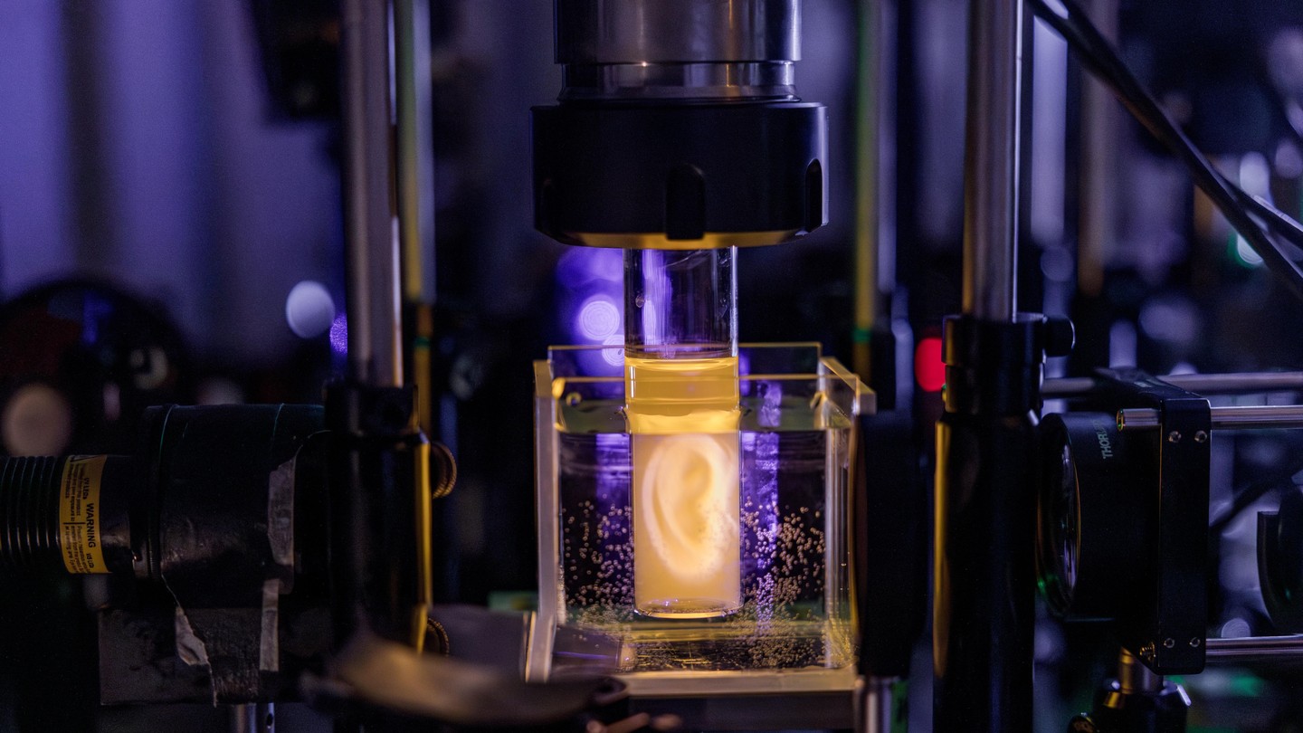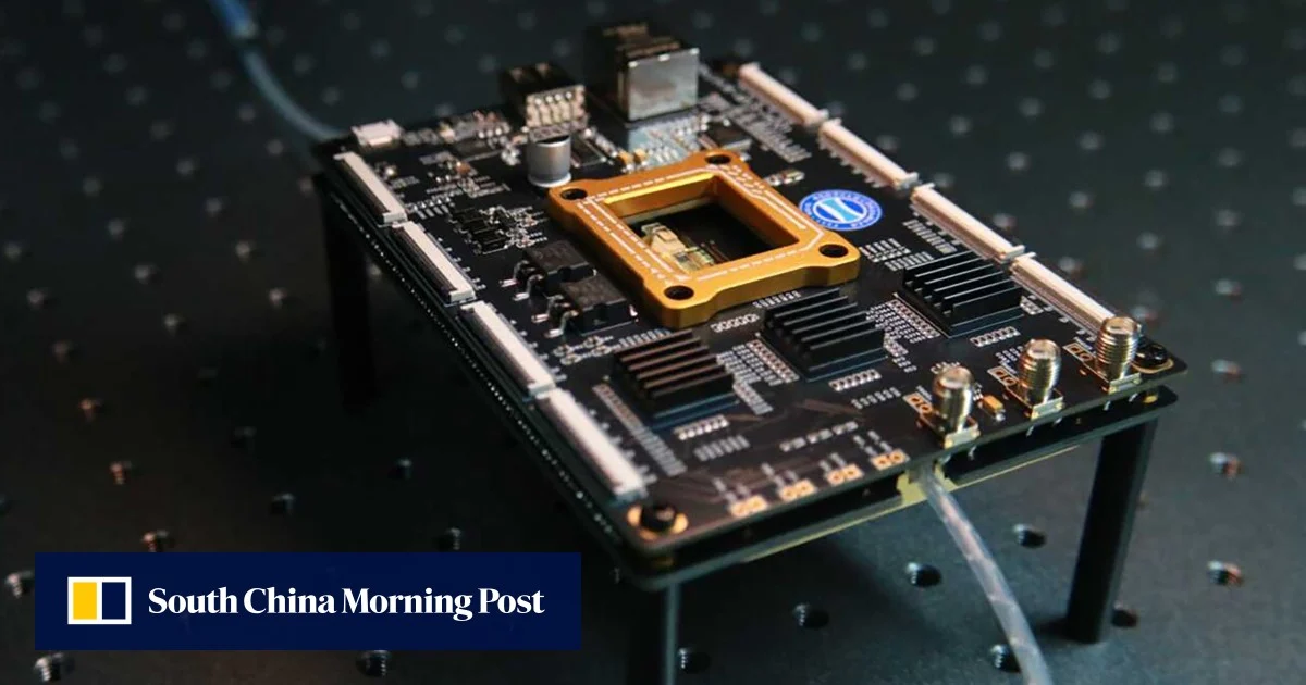
Using a new technique that can create vacancies at any site across a material and then shrink it to about 1/2,000 of its original volume, MIT researchers have designed nanotechnology devices that could be used for optical computing and other applications involving the manipulation of visible light.
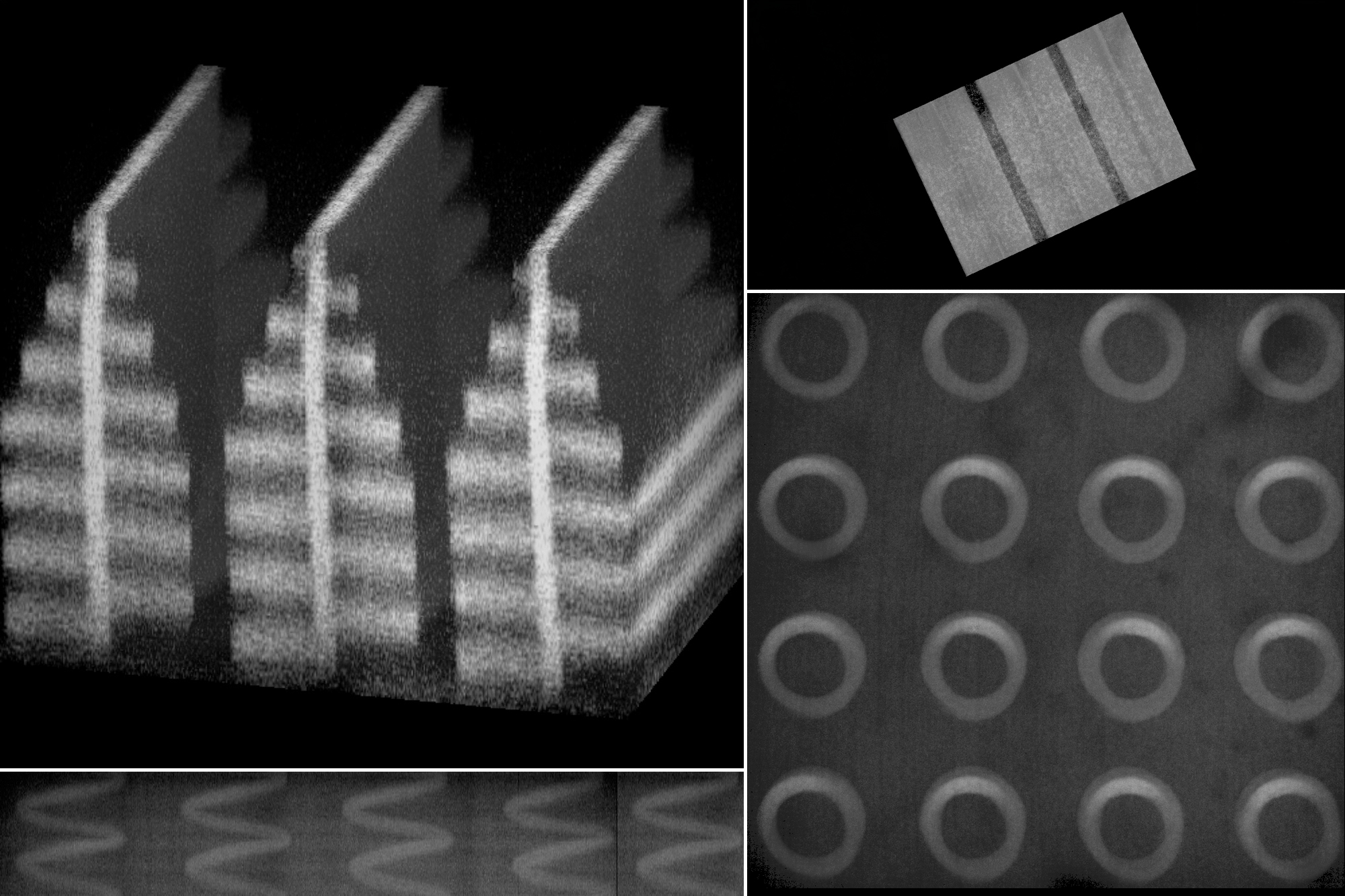
The new fabrication technique, known as “implosion carving,” allows researchers to imprint features throughout a hydrogel using photopatterning. If patterned with a resolution of about 800 nanometers, these features can then be shrunk to less than 100 nanometers.
Because that resolution is smaller than the wavelength of light, the devices can bend light in specific ways that allow them to perform optical computations.
MIT engineers created this photonic device by laser-patterning a hydrogel and then shrinking it to 1/2000 of its original volume.
“In order to enable nanophotonic applications in visible light, we need to make nanostructures with feature sizes with a resolution less than 100 nanometers. Only in that way can we precisely create the structure that can manipulate visible light,” says Quansan Yang, a former MIT postdoc, now an assistant professor at the University of Washington, and one of the lead authors of the new study.