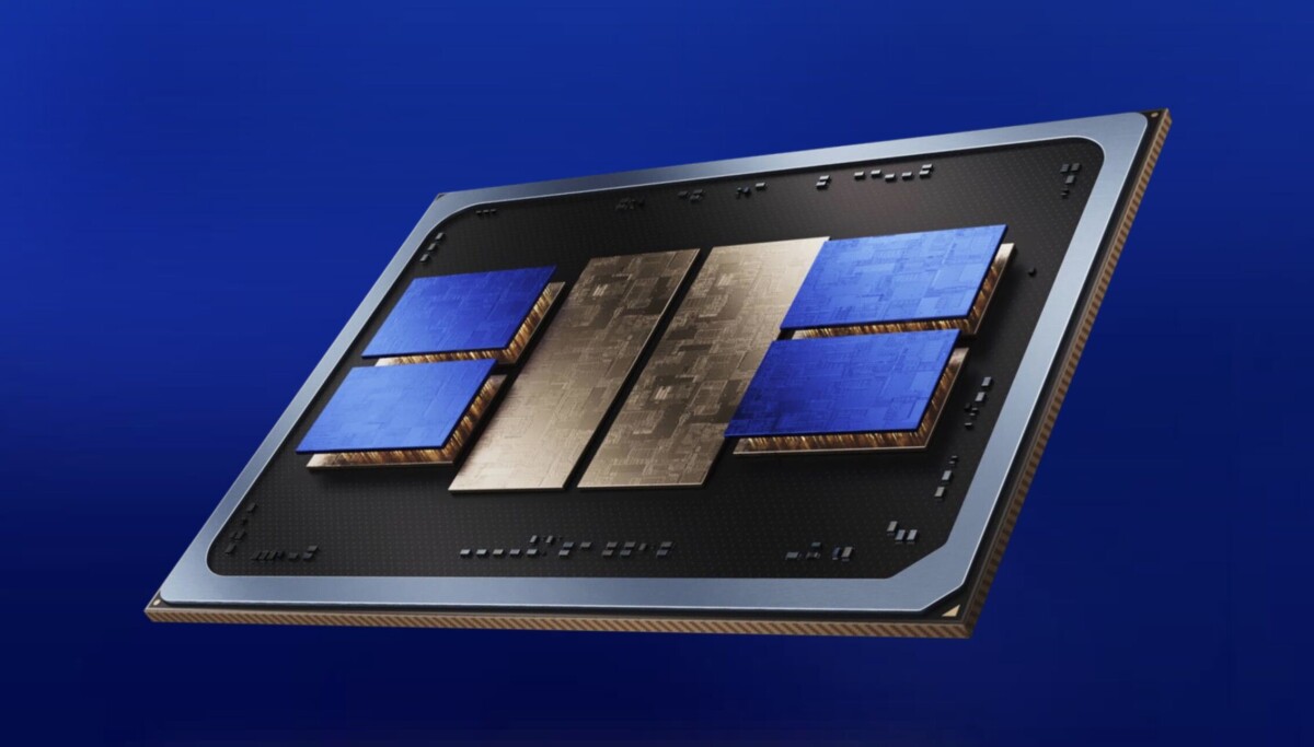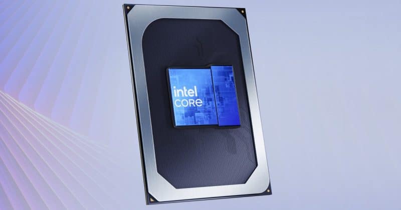
The semiconductor arms race just got a new battleground. Intel is developing a dual-sided power delivery architecture for its 14A2 process node, a design shift driven by the physics of cramming interconnects down to 21nm spacing. The move positions Intel directly against TSMC’s A14 and Samsung’s SF1.4 and SF2Z programs in what is shaping up to be the most consequential chipmaking competition in years.
Here’s the thing: when you shrink interconnect pitch to 21nm, the old way of routing power through the front side of a chip starts working against you. The wires that carry power compete for space with the wires that carry signals, and at 21nm, that tradeoff becomes untenable. Intel’s answer is to split the job across both sides of the chip.
What dual-sided power delivery actually means
Intel’s implementation will pair its PowerDirect BSPDN technology with front-side metal layers that handle signal and clock delivery. Power comes up from the bottom, data moves across the top, and the two systems stop tripping over each other.
Intel has already been developing BSPDN capability through its PowerVia technology on existing process nodes. The 14A2 program represents the first time that work gets integrated into a leading-edge production node at volume scale.