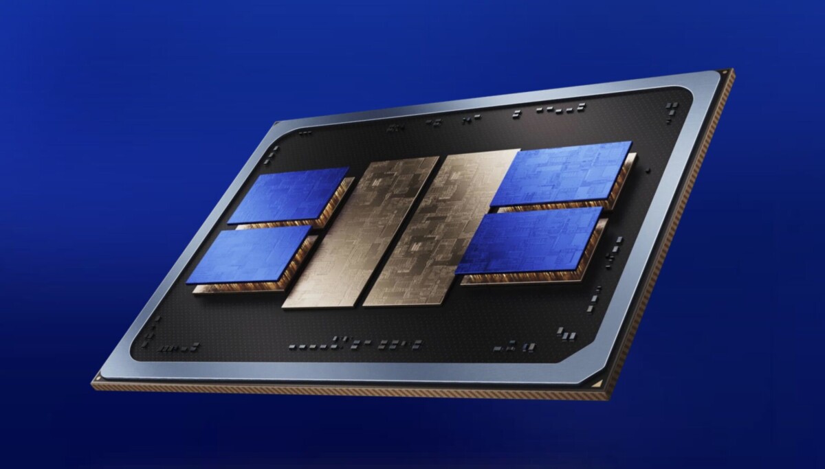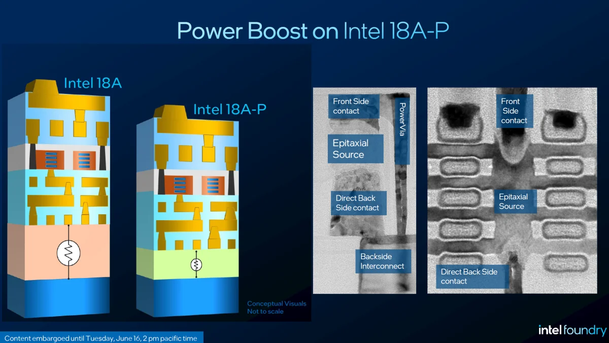
Intel 18A-P, the performance-tuned member of the 18A family that promises 9 per cent more speed at the same power or 18 per cent lower power at the same speed, entered risk production this week at the VLSI Symposium in Honolulu — on the timeline Intel set a year ago. That punctuality is the whole story. A foundry sells trust before it sells wafers, and trust gets built one met deadline at a time. The blueprint is sound now. Whether anyone signs a lease on the building is the question that decides Intel's next five years.Key TakeawaysIntel 18A-P has entered risk production, the trial stage before high-volume manufacturing, delivering 9 per cent higher performance at matched power or 18 per cent lower power at matched performance versus Intel 18A, with 20–40 per cent better thermal resistance.The node stays fully design-rule compatible with 18A, so a customer reuses existing chip designs and IP rather than redrawing them.Yield — the share of working chips per wafer — decides whether Intel converts marquee interest into signed volume. Industry estimates place 18A yield near 50–55 per cent against an estimated 65–70 per cent for TSMC's N2; treat both as estimates.A reported preliminary Apple agreement awaits confirmation from both companies. Entry-level Mac silicon is the likeliest first target if it lands.Elon Musk has named Intel's next node, 14A, for the full-scale build of Terafab, the Tesla–SpaceX–xAI chip-fab venture in Austin.What "risk production" actually meansRisk production is the trial run before the real thing. Intel commits a process to the fab, makes chips on it, and watches the defect rate — the customer accepts the "risk" that yields climb to volume-worthy levels before betting a product on them. For 18A-P, Intel says it reached that stage on schedule, the second milestone in a row the company has hit after a decade of slips that handed TSMC the manufacturing crown.The gains come from plumbing. Intel 18A moved power delivery to the back of the wafer — PowerVia, Intel's term for backside power — so the power lines stop competing with signal lines for room on the front. 18A-P extends that with Power Boost, a dual-contact transistor that draws current from both sides at once, lifting drive strength while holding capacitance flat. Naga Chandrasekaran, executive vice president and general manager of Intel Foundry, called the VLSI updates a signal that Intel stays committed to leading-edge process work "over the long term," and said the company appreciated the chance to share progress on a journey with road still ahead.Intel 18A → 18A-PGainPerformance at matched power9 per cent higherPower at matched performance18 per cent lowerThermal resistance20–40 per cent improvedVia resistance10–30 per cent improvedDesign-rule compatibilityFull reuse of 18A IPCell heights180nm and 160nmIntel has its eye in; the runs come laterYield is the number that governs everything from here. A process can read beautifully on a slide and still cost too much per working chip to win a customer, because every dead die on the wafer gets paid for by the live ones. Neil Shah, partner at Counterpoint Research, set the bar plainly: he said that if Intel can hold a yield above 90 per cent in the first month, it stands to win a few more customers. Today's reality sits well short of that mark.The scoreboard tells the harder truth. In the first quarter of 2026, TSMC booked $35.9 billion in foundry revenue. Intel Foundry booked $5.4 billion — and of that, roughly $174 million came from external customers, around 3 per cent. The rest was Intel making chips for Intel.Q1 2026 foundry revenueFigureTSMC$35.9 billionIntel Foundry, total$5.4 billionIntel Foundry, external customersapproximately $174 millionThat gap is the whole game. A batter can look set and walk back on 30; the runs that matter are the ones converted into a score the opposition has to chase. Intel has played itself in — the process works, the deadlines are landing, its own Panther Lake laptop chips and Xeon server parts ship on 18A. The patient, unglamorous work of pushing yield into the high numbers and turning a working line into a paying business is the innings that decides the match. Lip-Bu Tan, Intel's chief executive, has called 18A the most innovative process node in the company's history while admitting that scaling it with customer-grade consistency remains the central challenge.Will Apple actually move to Intel?Reporting points to a preliminary agreement for Intel to make some Apple chips, though both companies have stayed publicly silent, so treat it as likely-but-unconfirmed. The pull on Apple's side is real and recent. On Apple's most recent earnings call, chief executive Tim Cook told analysts the March-quarter supply squeeze "was primarily driven by the availability of the advanced nodes our SoCs are produced on" — Apple's A19 silicon and TSMC's 3nm line, the same line the AI-chip rush is draining. When demand outruns your single supplier, a credible second source stops being a cost question and becomes a survival one.Ben Bajarin of Creative Strategies reads Apple's position as exactly that capacity problem, arguing Intel is the only fab that can scale as a viable second source. His verdict on the deal itself: "I 100% believe this is going to happen. I don't know when." The likeliest first product is entry-level Mac silicon — the M-series chips in a MacBook Air or iPad Pro — at a volume one analyst estimate puts near 15–20 million units a year. Apple starting at the bottom of its own stack rather than the iPhone reads as sensible; you hand a new fab the chip you can afford to be patient with.The whole thing still hangs on the yield line. Apple runs the tightest product calendar in consumer electronics, and a fab that misses a tape-out or a ramp date costs more than any per-wafer saving it offers. Intel earns this customer by holding schedules, not by winning slideware.The $119 billion wildcard in AustinElon Musk has tied his chip ambitions to Intel: on Tesla's first-quarter earnings call he said the full-scale Terafab would run Intel's 14A process. Terafab — a Tesla, SpaceX and xAI venture launched in March at Austin's old Seaholm Power Plant — is meant to fold chip design, lithography, fabrication, memory and packaging under one roof. Musk called it "the most epic chip building exercise in history by far," and the numbers match the rhetoric: a SpaceX filing estimated $55 billion for the prototype fab and $119 billion across its phases, with analysts pricing the full-scale facility somewhere between $5 trillion and $13 trillion.Set that against what already stands. Intel's Arizona fab has been pouring 18A chips in high volume since December — concrete poured, building occupied, tenants moved in. Terafab is an architect's render at cathedral scale: roughly a hundred million square feet, about ten times Giga Texas, foundations yet to be dug. Even Musk has trimmed the near-term version to a research fab in Austin costing around $3 billion and managing a few thousand wafers a month, with SpaceX handling the first scaled phase.The skeptics have a point worth keeping. Building a fab is harder than building a rocket factory, and a realistic timeline runs three to five years even when everything breaks right. The strategic value lands earlier than the silicon, though. A credible Terafab hands Musk leverage over TSMC and Samsung on pricing and allocation, and it hands Intel a possible anchor tenant for expensive 14A capacity — plus a public vote of confidence in the node that follows 18A.India's foundations, and the climb above themAn Intel that can credibly second-source TSMC strengthens the exact argument India keeps making in Washington — that the world's advanced chips sit too concentrated in one set of fabs on one island. India's pitch is the "China plus one" supply story, and every new leading-edge alternative to TSMC validates the diversification logic India is selling.The honest read also measures the distance. India Semiconductor Mission 2.0, launched in the 2026–27 Union Budget with a Rs 8,000 crore single-year outlay inside a Rs 76,000 crore framework, has shifted focus from luring fabs to building equipment, materials and design IP, with fiscal support up to 50 per cent of project cost. The flagship build, the Tata Electronics–PSMC fab at Dholera, is a roughly Rs 91,000 crore project running mature nodes at 50,000 wafers a month, targeting first silicon late this year; Micron's Sanand packaging plant came online in February. All of it sits at 28nm and packaging — foundations being laid while Intel and TSMC contest the top of the order at 2nm and below. India aims for 70–75 per cent domestic self-sufficiency by 2029 and 2nm-class capability only by 2035. The Intel story is a useful mirror: it shows both the prize and the years of climbing between footing and frontier.The clause that matters in the second halfWatch one sentence, not the spec sheet. Tan has said he expects commitments from multiple foundry customers in the second half of 2026, and that promise is the real examination — the physics question got answered this week in Honolulu. The blueprint is approved. The show home is built and lived in, Intel's own chips proving the line runs. What Intel needs now is signatures on the lease: Apple's name above the door, Musk's deposit on 14A, a roster that converts $174 million of external revenue into something that bends the TSMC gap. A node can be the finest thing on paper and still stand empty. By the time the H2 earnings calls land, the question moves from whether 18A-P works to who pays Intel to run it.FAQWhat is Intel 18A-P?It is a performance-enhanced version of Intel's 18A manufacturing process, a 2nm-class node. Against 18A it offers 9 per cent higher performance at the same power or 18 per cent lower power at the same performance, plus better thermals, and it reuses existing 18A chip designs without a redraw.What does "risk production" mean?It is the trial manufacturing stage before high-volume production. Intel makes chips on the process and refines the yield; a customer takes the early "risk" that output climbs to commercially viable levels. It signals the node is real and on schedule, ahead of mass production.Is Apple definitely shifting chips to Intel?No confirmation exists from either company. Reporting describes a preliminary agreement, most likely starting with entry-level Mac silicon, but Apple and Intel have both stayed publicly silent. The decision is widely expected to ride on Intel's yields holding up.How is Intel connected to Elon Musk's Terafab?On Tesla's Q1 2026 earnings call, Musk said the full-scale Terafab fab in Austin would use Intel's next-generation 14A process. Terafab is a Tesla–SpaceX–xAI venture; near-term plans centre on a roughly $3 billion research fab, with far larger phases estimated in the tens to hundreds of billions.How does Intel 18A-P compare with TSMC's 2nm?On paper they are close, and Intel shipped backside power delivery in volume with 18A ahead of TSMC's equivalent Super Power Rail, which arrives with N2P and A16. TSMC's edge is execution: its N2 entered volume production in late 2025, and its yields are estimated higher than Intel's. Yield and consistency, rather than headline specs, separate them today.end of article
Why Intel's 18A-P Milestone Matters for Apple, Tesla and TSMC
Intel's new 18A-P chip technology has entered a trial production phase. This marks a significant step for Intel Foundry's future. The company aims to secure major clients like Apple and Elon Musk's Terafab project. Success hinges on achieving high production yields. This development is critical for Intel to gain market share against rivals like TSMC.
1,853 words~8 min read