Insider Brief
ETH Zurich researchers developed a technique that uses trapped ions to create high-resolution three-dimensional maps of electric and magnetic fields near quantum chips, helping identify sources of noise that limit quantum device performance.
The team used a Penning ion trap to move a single beryllium ion in three dimensions and achieved a record sensitivity by detecting oscillating electric fields as small as 10 nanovolts per meter in one second.
The method could help researchers evaluate chip materials, reduce electromagnetic interference and improve the performance of future quantum computers and quantum sensors.
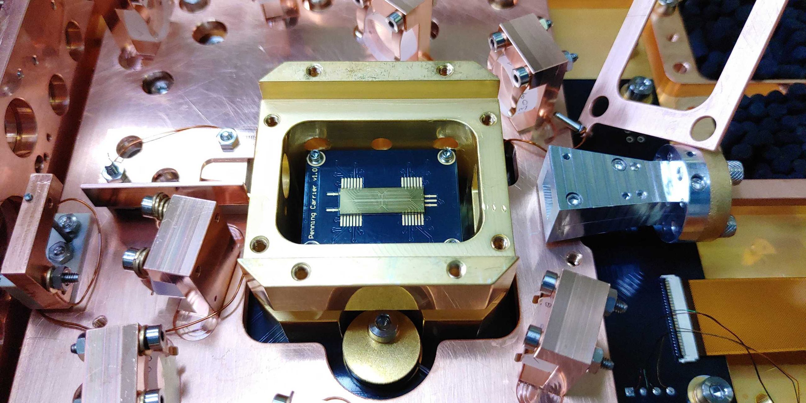
PRESS RELEASE — Single electrically charged atoms – ions – have been successfully used for some time as quantum bits in quantum computers and quantum sensors. Unlike the bulky ion traps of the early years, there are now miniaturised chips in which ions can be trapped and manipulated only a hair’s breadth above the surface of the chip. This has many advantages, but also one decisive drawback: noisy electromagnetic fields coming from the chip itself can severely impair the sensitive quantum states of the ions and hence the performance of the computer or sensor.