Soitec, one of France’s most important semiconductor companies, just locked in a strategic partnership with Chinese specialty foundry ZenSemi to ramp up high-volume production of advanced power chip technology. The deal centers on 300mm BCD-on-SOI substrates, which is a mouthful that translates to: the specialized silicon wafers that make power management chips smaller, faster, and more energy-efficient.
What the deal actually involves
The collaboration focuses on scaling production of what’s called BCD-on-SOI technology. BCD stands for Bipolar-CMOS-DMOS, a process that combines three different transistor types onto a single chip. SOI, or Silicon-on-Insulator, is Soitec’s bread and butter: an engineered substrate technique that adds an insulating layer to reduce power leakage and boost performance.
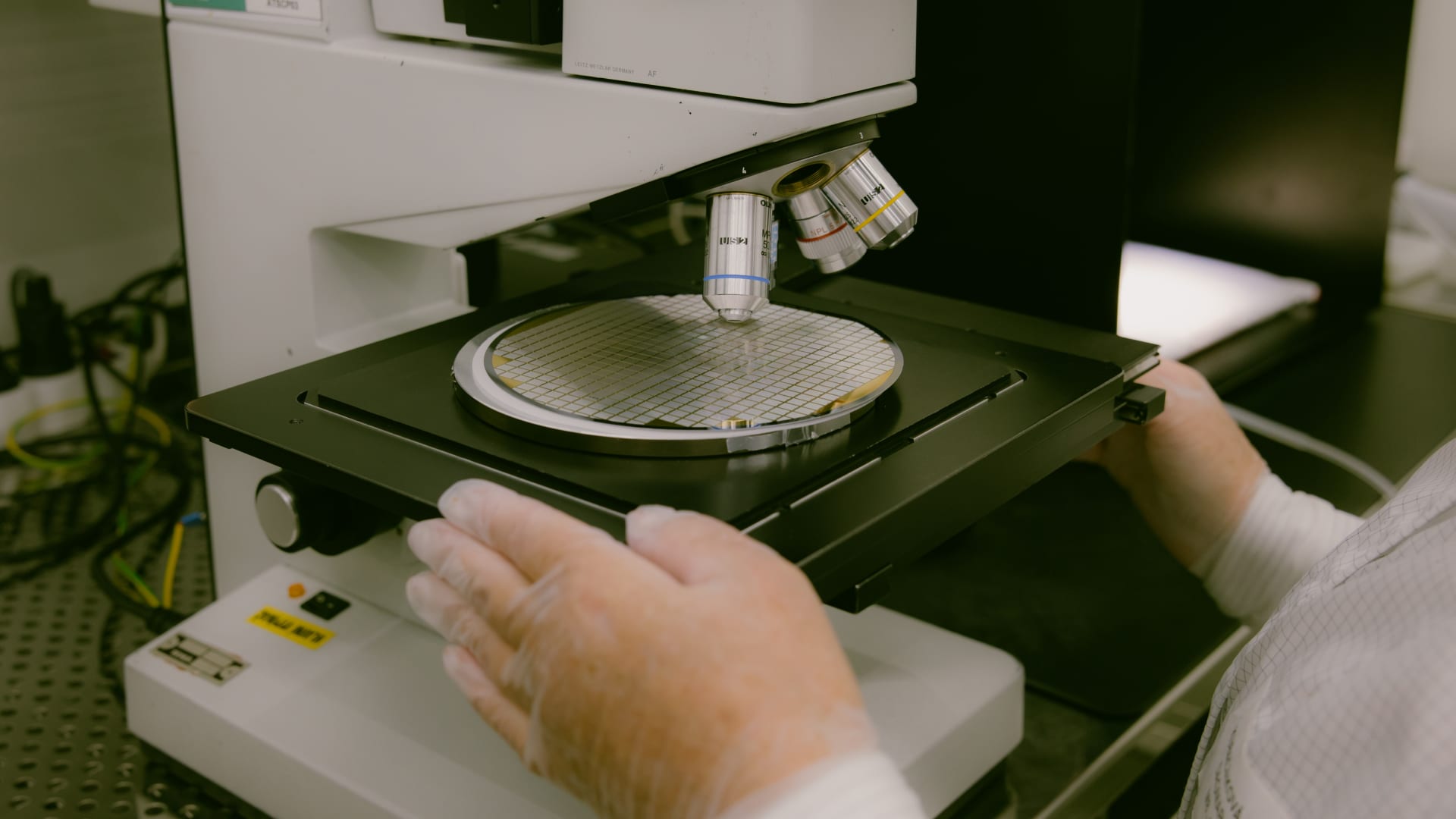
Soitec will supply its 300mm Power-SOI substrates to ZenSemi, which will use them to develop new manufacturing processes and expand its production capacity. The 300mm wafer size matters because it’s the industry standard for high-volume manufacturing. Bigger wafers mean more chips per production run, which means lower costs per unit.
The target applications include AI datacenters, electric vehicles, humanoid robots, and industrial systems. Soitec brings serious intellectual property to this arrangement. The company holds over 4,800 active patents, most of them related to its engineered substrate technologies.