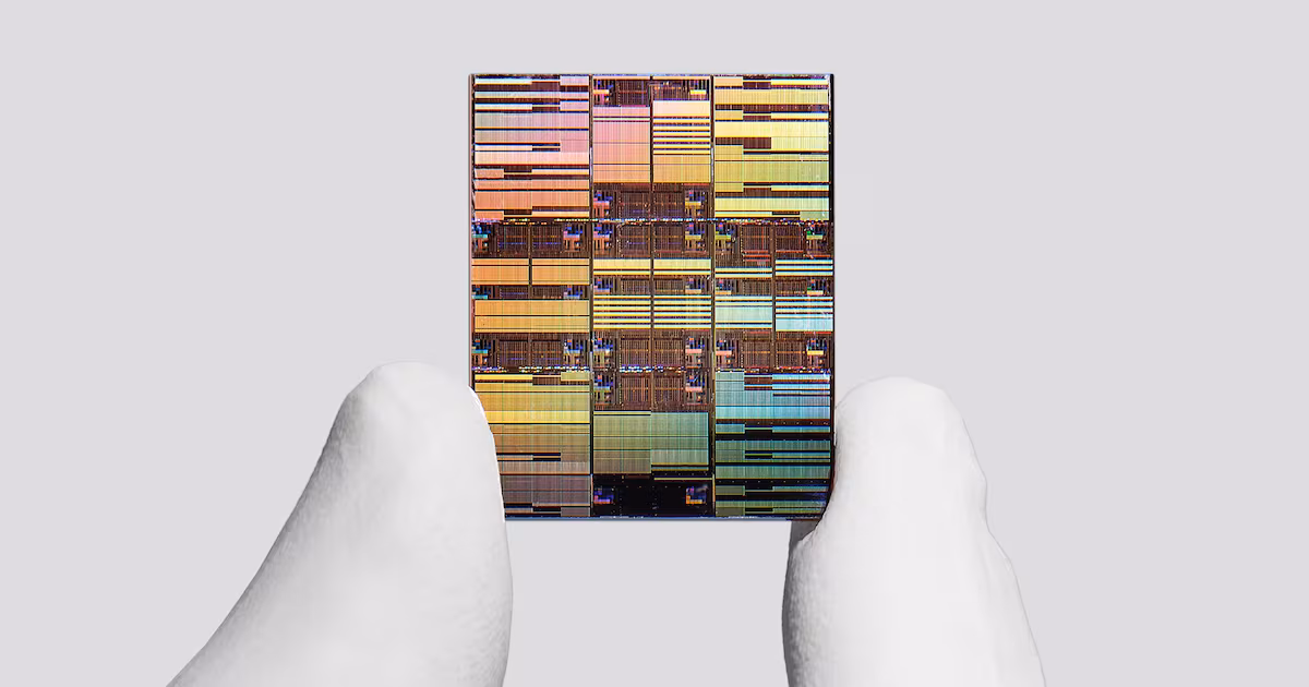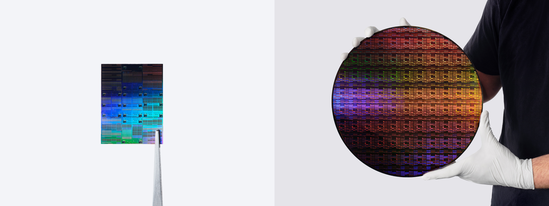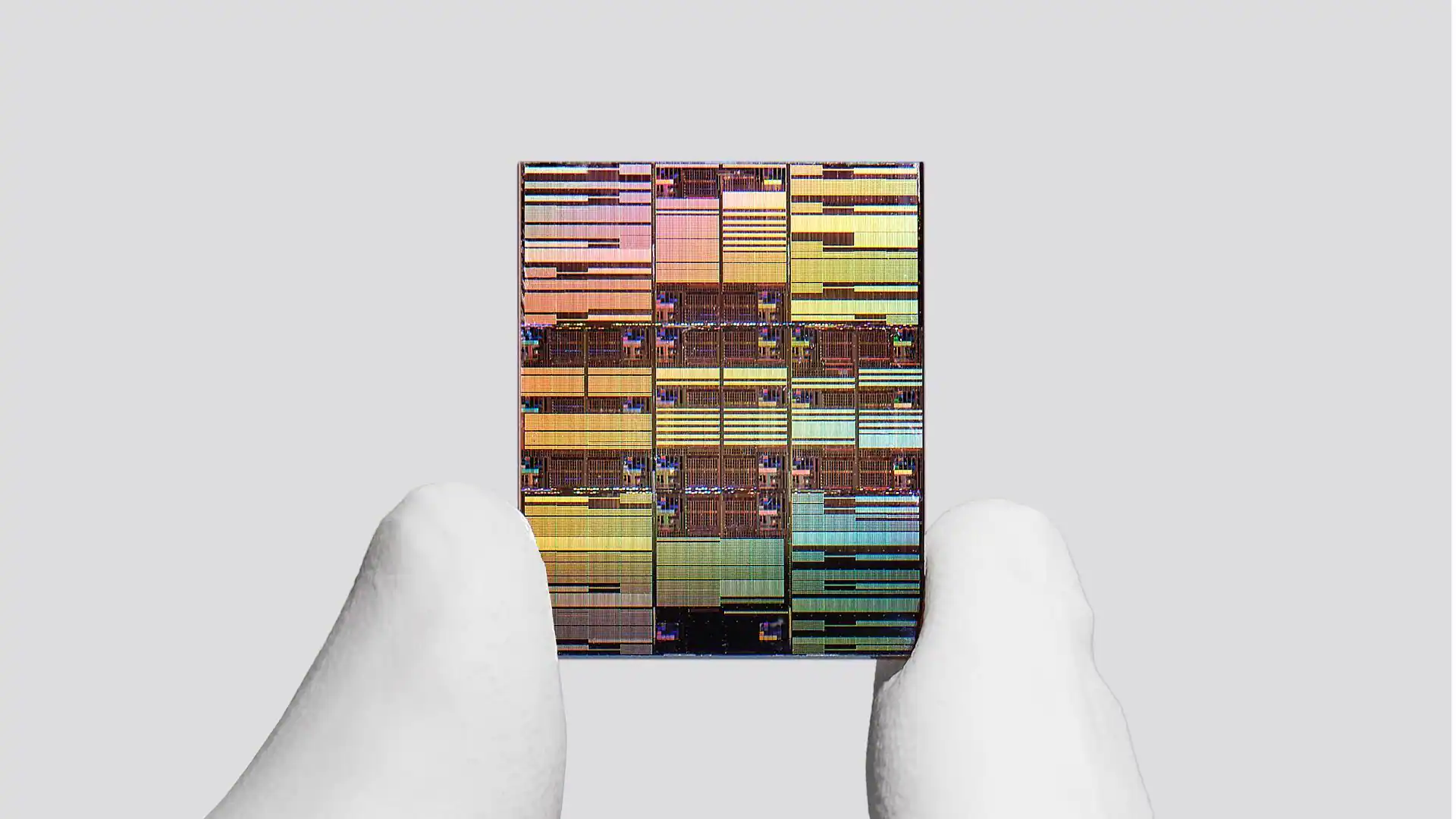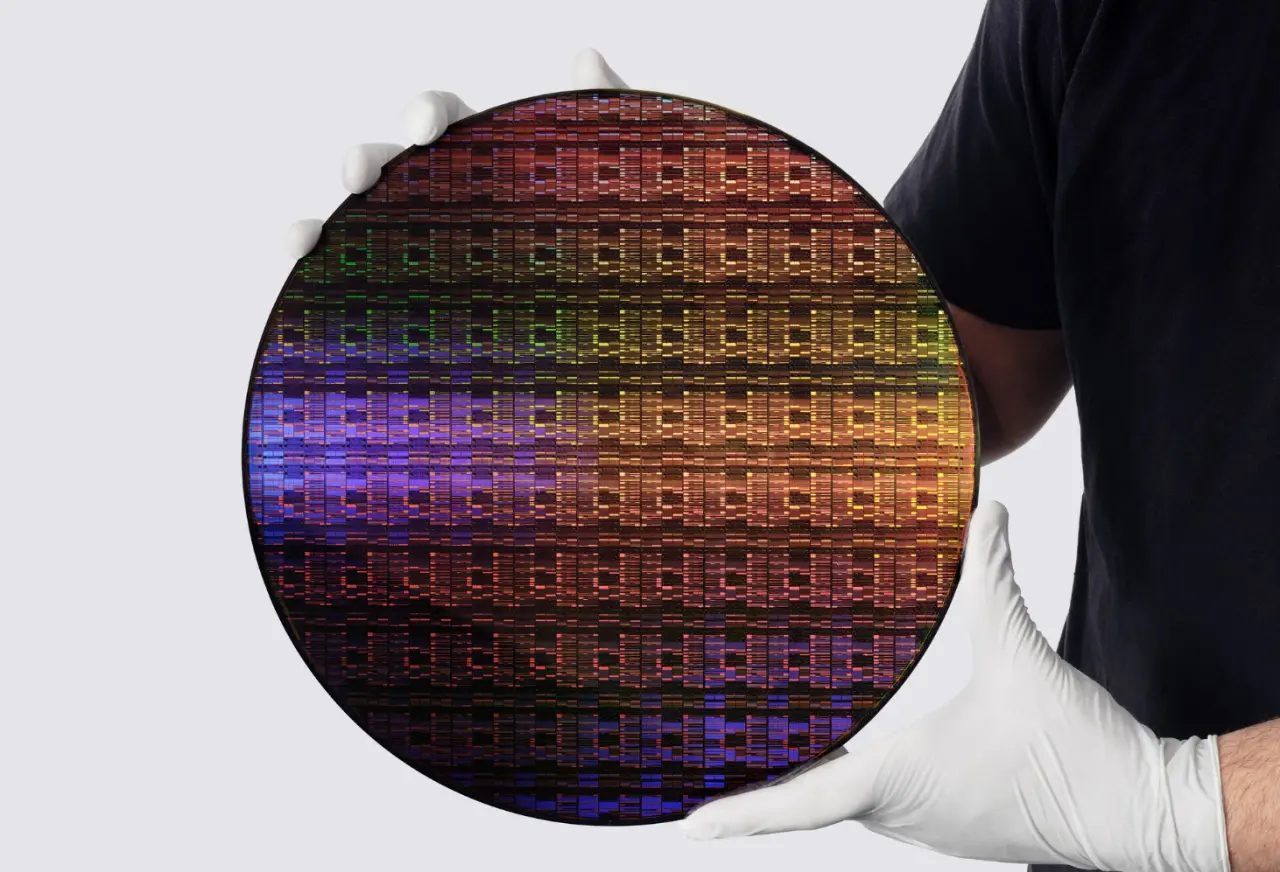
In a major breakthrough, IBM revealed the world’s first semiconductor chip technology built on a sub-1 nanometer chipmaking process. For comparison, the process uses transistor features smaller than the width of a DNA strand, which measures about 2.5 nanometers across. The chip itself is about the size of a fingernail but holds almost 100 billion transistors, and the company expects it could enter markets as early as the next five years. In a statement released today, IBM said the new chip features nearly twice the density of its 2-nanometer chip, released in 2021. According to an accompanying technical report, the chip also demonstrated up to 70% greater energy efficiency than its predecessor. In designing the chip, researchers developed an “entirely new transistor architecture” called nanostack, which “vertically stacks and staggers transistors” to enable IBM’s 0.7-nanometer chip technology, IBM explained. A section of the chip seen with a transmission electron microscope. Credit: IBM “With our new nanostack architecture, we’re not just making smaller transistors,” Jay Gambetta, director of IBM Research, said in the statement. “We’re reinventing how chips are built to deliver dramatically more power and energy efficiency.”
IBM Crosses One of Computing's Biggest Barriers With World's First Sub-1 Nanometer Chip
The new chip technology packs nearly 100 billion transistors into a fingernail-sized chip.
555 words~3 min read