00:00/00:00
您的浏览器不支持 audio 标签。
Listen to this article
1x
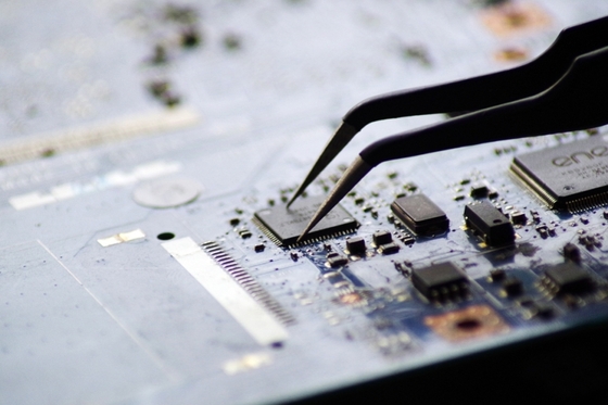
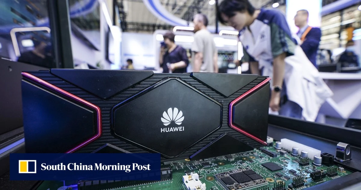
Huawei Technologies Co. Ltd. recently threw a conceptual bombshell into the global semiconductor industry, unveiling the Tau (τ) Scaling Law as a radical paradigm for chip design.
The tech giant’s embrace of a 3D architecture reflects where the global semiconductor industry is already headed, though turning the concept into commercially viable products remains a formidable challenge
00:00/00:00
您的浏览器不支持 audio 标签。
Listen to this article
1x
Huawei Technologies Co. Ltd. recently threw a conceptual bombshell into the global semiconductor industry, unveiling the Tau (τ) Scaling Law as a radical paradigm for chip design.
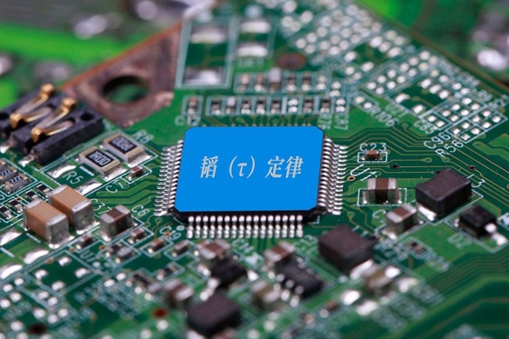
Tau Law aims to reduce latency and raise energy efficiency through LogicFolding and optical interconnects. The question is…

Unitree fast-tracks Shanghai IPO with target valuation of $6.2 billion, DeepSeek cuts flagship AI model prices by 75% as funding…
The Chinese tech giant said its “Tau Scaling Law” can boost chip efficiency through vertically stacked circuit design
Huawei's Tau Scaling Law and LogicFolding 3D architecture aim to bypass US sanctions by rethinking chip design, targeting…
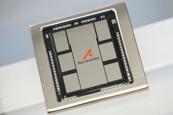
Company says 3D design can deliver world-beating chips without the best chipmaking gear, rewriting the playbook for China’s tech…

While China's semiconductor industry navigates intensified trade hurdles and narrows the gap with global competitors, a newly…