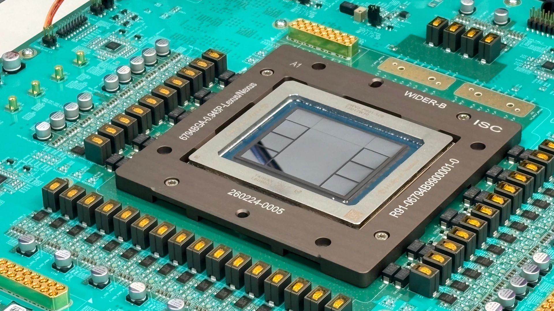
Arm Holdings and Samsung Electronics are teaming up to build next-generation AI chips using Samsung’s 2nm manufacturing process. Arm approved the non-recurring engineering fees for the project at the end of August 2026, officially kicking off the joint R&D effort.
Arm’s stock climbed roughly 2.5–3% on the news.
What they’re actually building
The collaboration is focused on developing system-on-chips, or SoCs, purpose-built for on-device AI. The division of labor is straightforward. Arm brings its AI accelerator architecture and register-transfer level design expertise. Samsung’s System LSI division handles SoC design and integration using Arm’s intellectual property. Samsung’s Foundry division takes care of manufacturing, advanced packaging, and commercialization.
The chips will be fabricated on Samsung’s 2nm Gate-All-Around, or GAA, process node. GAA is the successor to FinFET transistor architecture, which has dominated chipmaking for over a decade. The basic idea: instead of the gate wrapping around three sides of a transistor channel, GAA wraps around all four. That gives chipmakers better control over electrical current, which translates to lower power consumption and higher performance at smaller scales.