(Image credit: Nvidia)
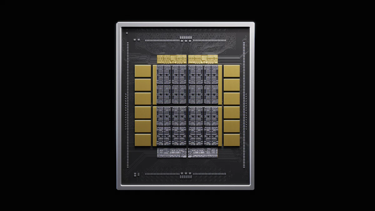
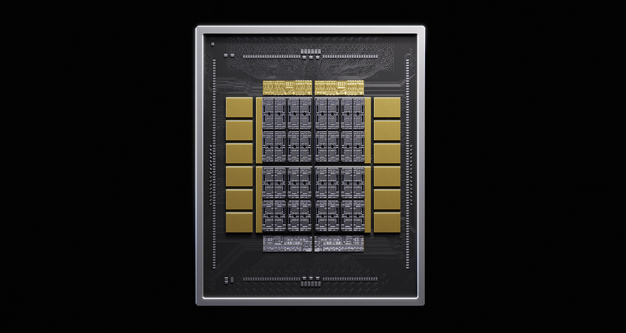
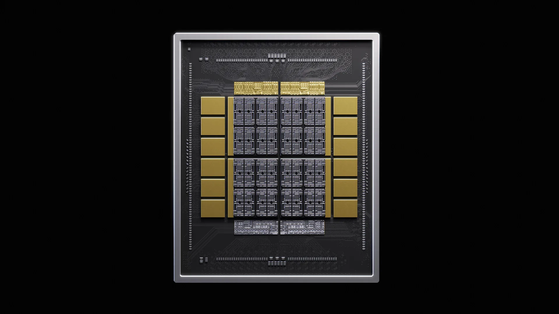
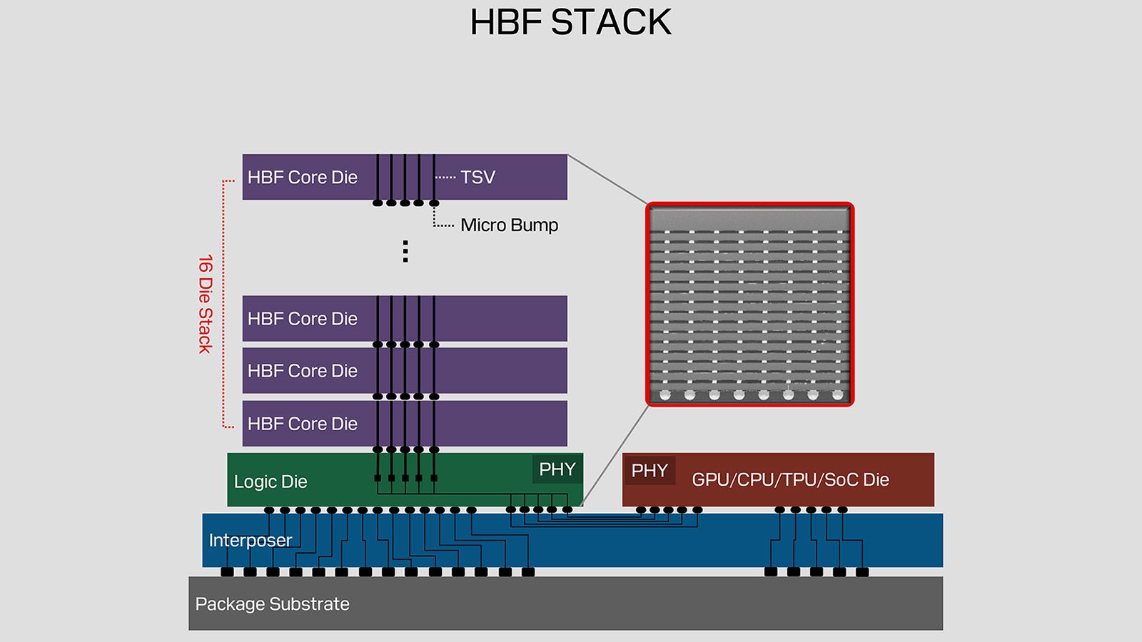
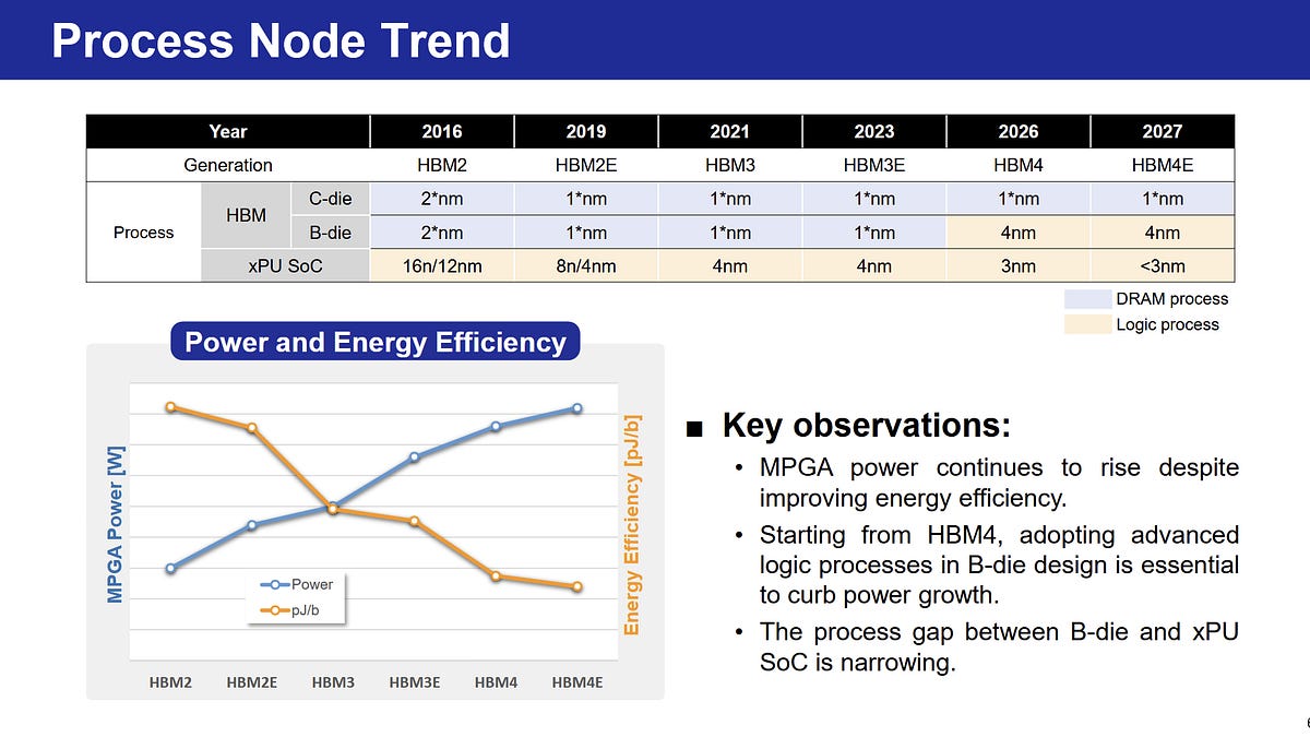
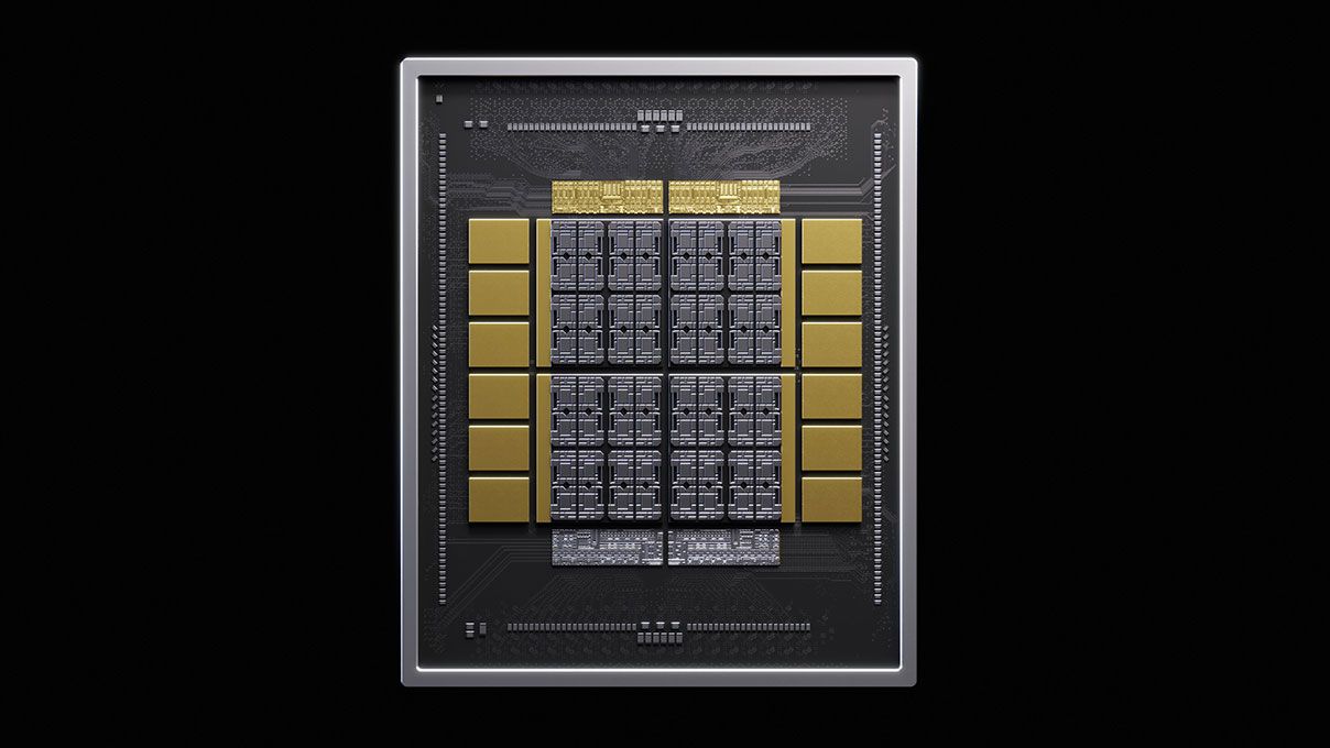
Nvidia's NVLink Fusion program gives the company's partners the building blocks necessary to connect custom chips with the NVLink scale-up domain used to join many separate processors into a single coherent system like the Vera Rubin NVL72 rack-scale accelerator. Today, Nvidia is adding a new building block to that toolkit: NVHBM, a custom implementation of the high-bandwidth memory that underpins practically every AI accelerator in use today.Go deeper with TH Premium: MemoryAs Nvidia describes it, NVHBM is a custom HBM base die that promises higher bandwidth, lower power usage, and a smaller on-die footprint than traditional HBM4e. Nvidia says it's designed and validated with "leading memory vendors," so it promises custom silicon developers faster time-to-market than implementing commodity HBM from the ground up. But it's worth re-emphasizing that this isn't an HBM replacement. Instead, it's a new building block that Nvidia is only offering to its custom silicon partners.Memory bandwidth is everything for AI accelerators, and NVHBM promises up to 30% higher bandwidth per stack than standard HBM4e. For memory-bandwidth-bound AI workloads, that higher bandwidth translates into higher throughput, such as a higher tokens-per-second rate for AI inference.The custom NVHBM base die also reduces the footprint of memory-related circuitry on the main custom accelerator die. Traditionally, the HBM memory controller has been incorporated into the primary silicon die on the package. NVHBM instead moves the memory controller into the base die of the HBM stack and provides a smaller custom PHY that NVLink Fusion customers can then integrate into their designs.