(Image credit: Fujitsu)
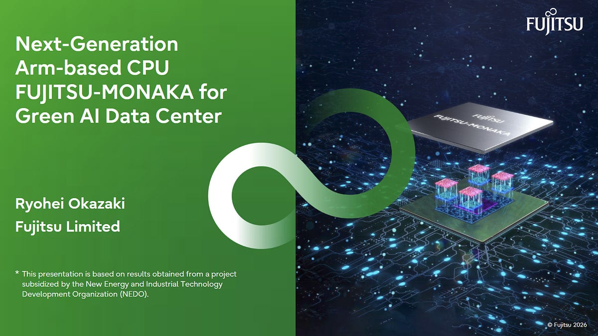
This Tom's Hardware Premium article is free to read with a Tom's Hardware account; no payment necessary. We're offering free access from August 23 to 26 so you can read all of our reporting from Hot Chips.Fujitsu gave us a detailed look at its 144-core Monaka server CPU at Hot Chips 2026 on August 24, confirming for the first time that the Arm chip runs dual 256-bit SVE2 vector units, down from the 512-bit SVE in its A64FX predecessor, and that its entire last-level cache sits on a separate 5nm die beneath the 2nm compute die.Ryohei Okazaki, lead architect of Fujitsu's processor development team, presented the design as "a made-in-Japan CPU, specifically engineered for AI performance and power efficiency," built for what the company calls green AI data centers and subsidized by Japan's New Energy and Industrial Technology Development Organization. The chip ships in two SKUs: a 350W air-cooled part at 2.1 GHz base and a 500W liquid-cooled part at 2.9 GHz base, with evaluation samples available now and volume production in 2027.
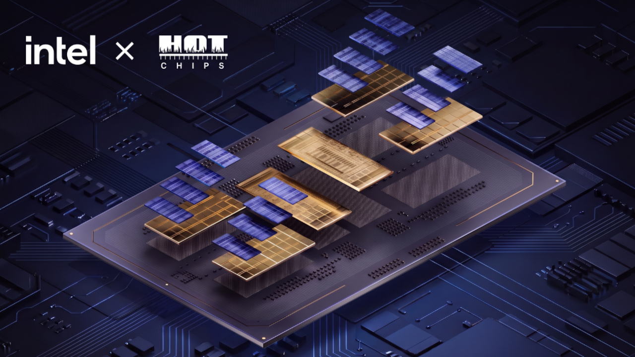
(Image credit: Fujitsu)Three dies, one stackMonaka splits into three tiers of silicon: a 2nm core die on TSMC N2P, a 5nm SRAM die on TSMC N5 that holds the whole last-level cache, and a 5nm IO die. The core die stacks face-to-face on top of the SRAM die through hybrid bonding, sitting on the cooling side because it runs hottest, while the IO die connects to the SRAM die across a silicon interposer. Fujitsu keeps 2nm silicon under 30% of total die area, a split Okazaki said lets Fujitsu "accelerate the time to market for our 2-nanometer-based chip" by pushing everything that shrinks poorly onto the 5nm SRAM and IO dies.