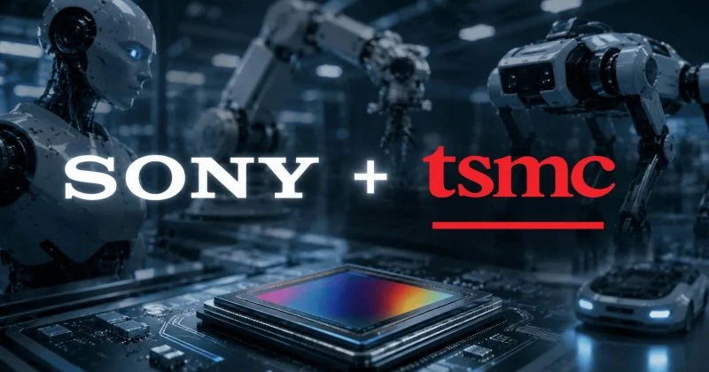
Two of the most important companies in the semiconductor food chain just decided to get even closer. Sony Semiconductor Solutions and TSMC signed a non-binding memorandum of understanding on May 8, 2026 to form a joint venture focused on developing and manufacturing next-generation image sensors, with mass production targeted for around 2029.
Sony will hold a controlling interest in the venture, which plans to build out development and production lines at a newly constructed fabrication facility in Koshi City, Kumamoto Prefecture, Japan. The goal: build sensors advanced enough to power what the companies are calling “physical AI” applications, think autonomous vehicles, industrial robotics, and whatever else needs machine eyes sharp enough to navigate the real world.
Why these two, and why now
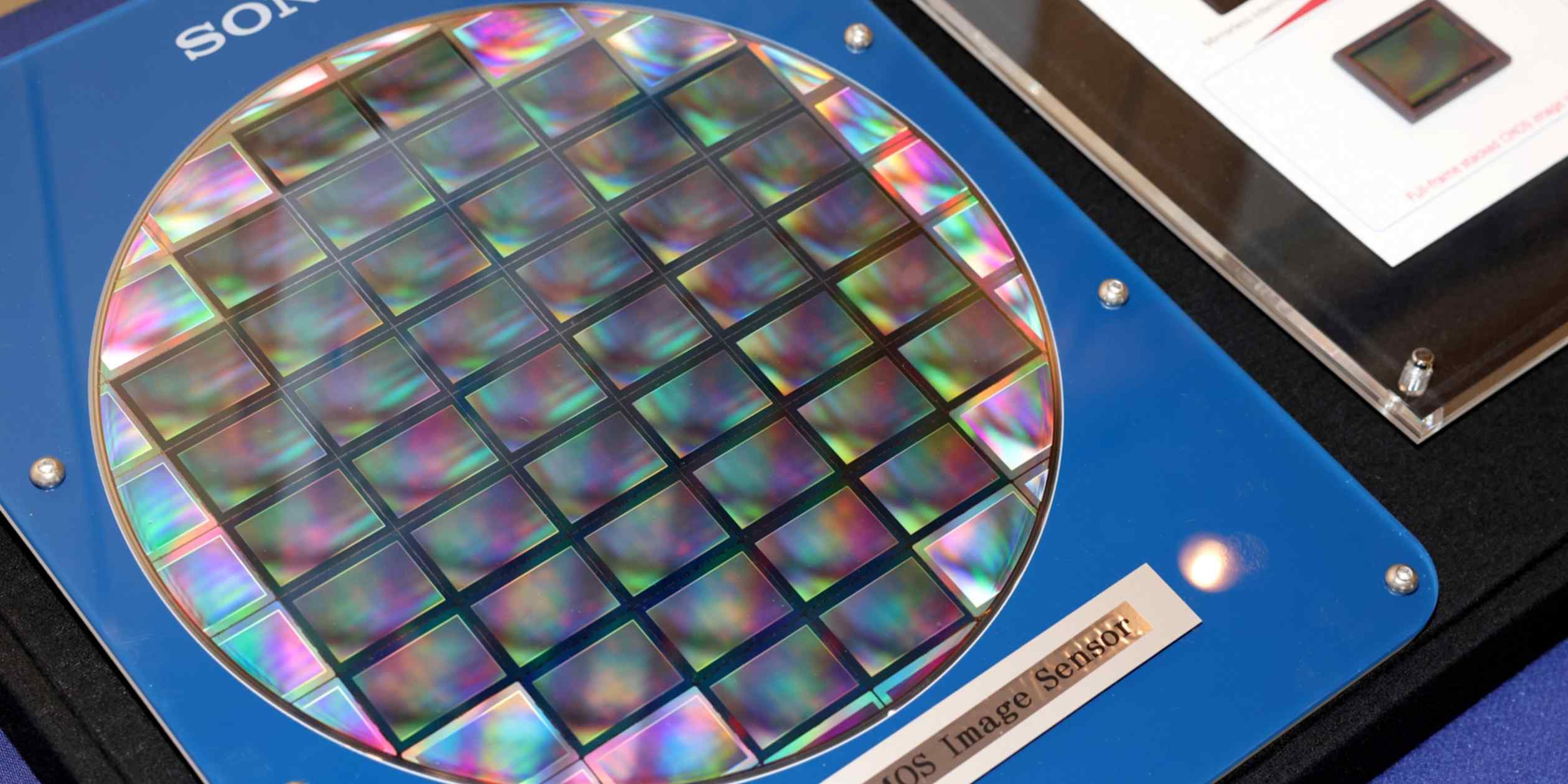
Sony and TSMC aren’t exactly strangers. The two companies have collaborated on CMOS image sensors for years, with Sony designing the sensors and TSMC handling the manufacturing. Sony already dominates the image sensor market, supplying the tiny silicon rectangles that let smartphones, security cameras, and cars see their surroundings. TSMC, meanwhile, is the world’s most advanced contract chipmaker, the company that builds processors for Apple, Nvidia, and most of the tech industry.