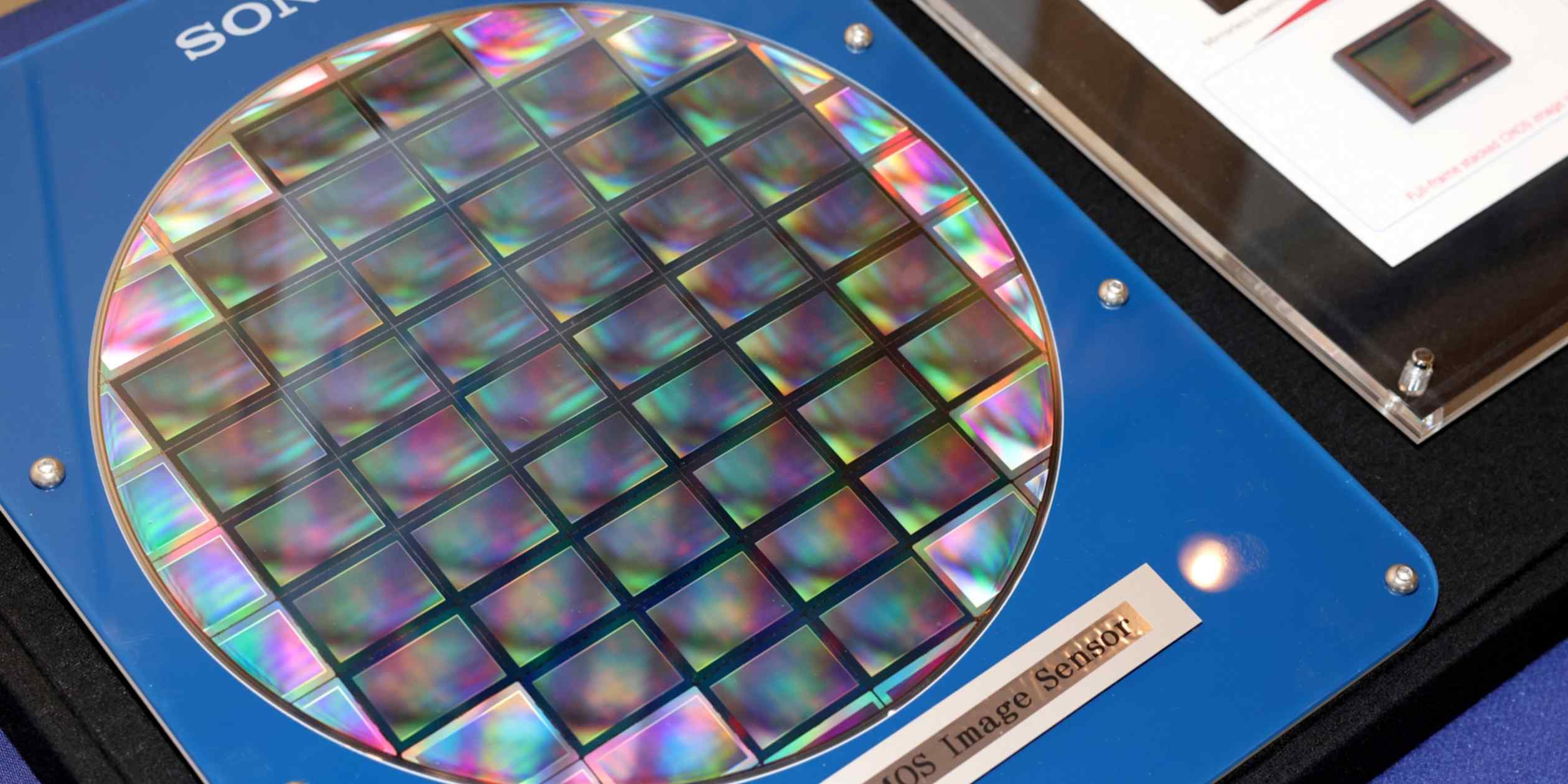
Two of the biggest names in chips are joining forces on the humble camera sensor. Sony and TSMC plan to spend around ¥1 trillion, roughly $6.4bn, on a joint plant in Japan to make the next generation of image sensors.
The logic of the pairing is easy to see once you know what each brings. Sony is the world’s leading designer of image sensors, the chips that turn light into the photos your phone takes, while TSMC is the world’s largest contract chipmaker, so the deal marries unrivalled design with unrivalled manufacturing.
The factory will rise in Kumamoto, in southern Japan, which is no accident. TSMC already runs advanced operations in the prefecture, so building there lets the partners tap an existing cluster of skilled workers, suppliers and infrastructure rather than starting from scratch.
Ownership tilts toward Sony, as you might expect given whose product this ultimately is. Sony will hold roughly 60% of the venture and TSMC about 40%, with commercial production targeted to begin as early as 2029, a timeline that reflects just how long leading-edge fabs take to build and qualify.
The reason to invest now is that image sensors are quietly becoming more valuable, not less. They already sit in every smartphone, but demand is spreading fast into cars, where sensors feed driver-assistance and autonomous systems, and into the broader world of physical AI.