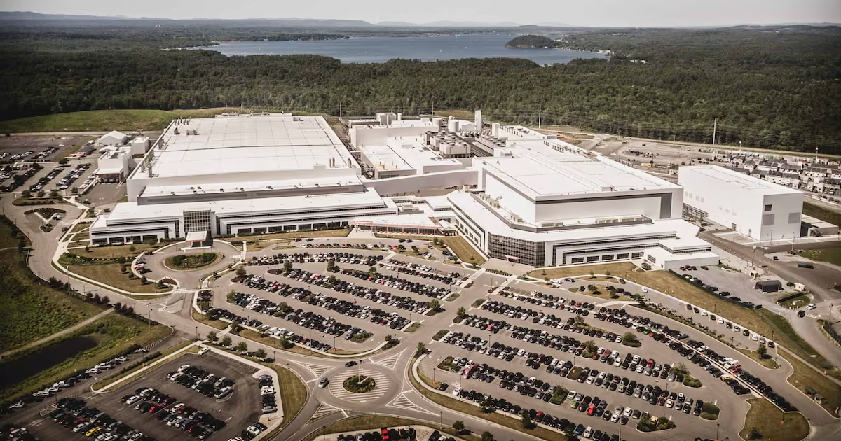
Insider Brief
GlobalFoundries has signed a letter of intent with the U.S. Department of Commerce for a potential $300 million CHIPS R&D award to advance silicon photonics technologies and advanced packaging.
The funding would support development of optical materials, wafer technologies, and manufacturing capabilities for near-packaged optics and co-packaged optics used in AI and high-performance computing systems.
GlobalFoundries will build on its silicon photonics platform and SCALE™ technology to expand U.S.-based production capabilities for next-generation optical interconnects.
Press release – GlobalFoundries (Nasdaq: GFS) today announced it has entered into a letter of intent (LOI) with the U.S. Department of Commerce to accelerate research and development of next-generation silicon photonics – the optical technology that moves data at the speed of light and underpins the AI and high-performance computing data centers driving the global economy. Under the LOI, the Department’s CHIPS Research and Development Office is expected to award GF $300 million to advance next-generation optical materials, wafer technologies and advanced packaging, reinforcing U.S. leadership in a technology essential to AI infrastructure.