(Image credit: AMD)
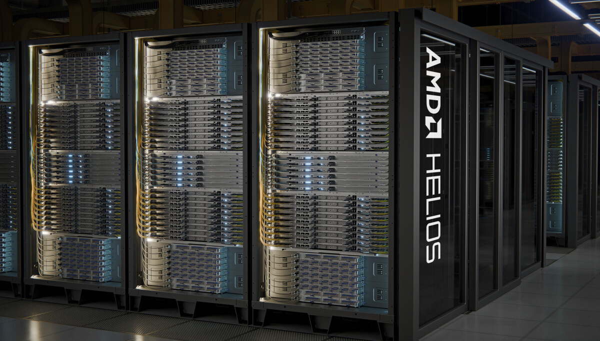
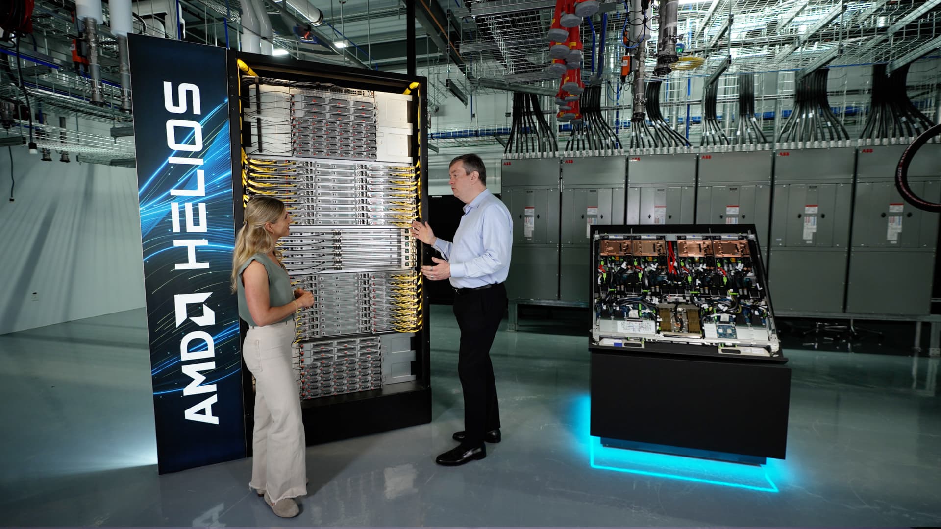
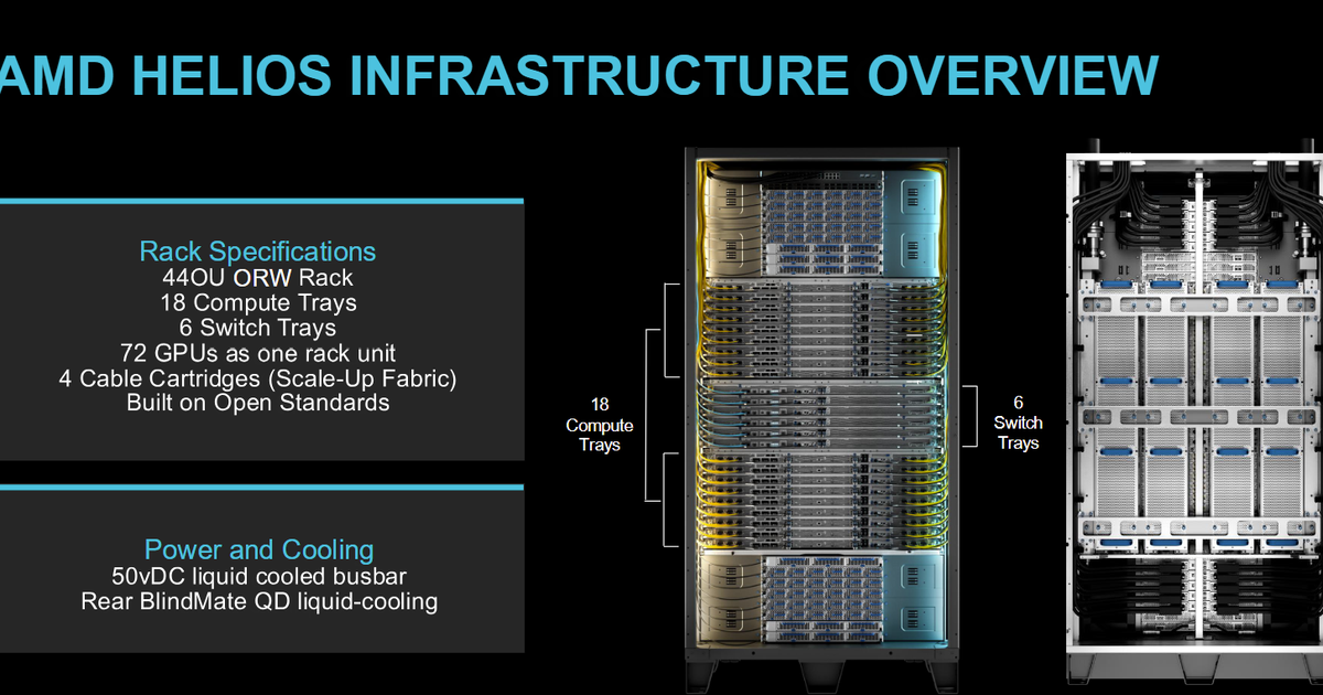
At AMD’s Advancing AI event this week, the company revealed more details of its upcoming MI455X GPU and the Helios rack-scale architecture that will join 72 of those GPUs into a coherent accelerator—the largest such system that AMD has built so far and its first to truly compete with Nvidia’s NVL72 rack-scale design, as used in the Blackwell and Rubin generations.AMD calls the MI455X “by leaps and bounds the most advanced AI accelerator we’ve ever built,” and from what we’ve seen, it’s the most competitive product at both the chip level and at rack scale that AMD has ever put up against Nvidia’s thorough dominance of the AI compute race.
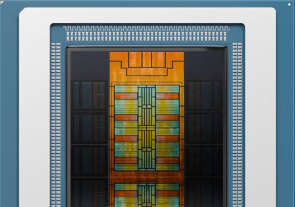
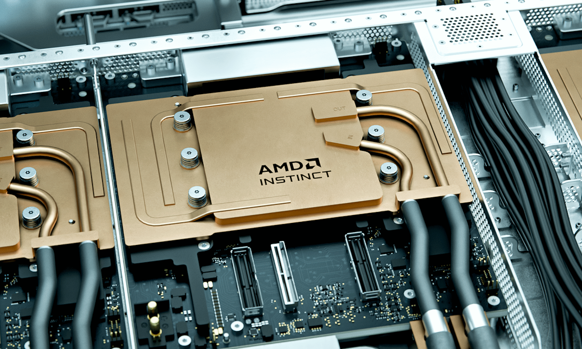
(Image credit: AMD)The full MI455X GPU is a massive chip encompassing 320 billion transistors, and it’s built up using advanced packaging technologies. Four Accelerator Complex Dies (XCDs) are stacked on top of each Fabric and Cache Die (FCD) using hybrid bonding. In turn, the two FCDs are each joined to six stacks of HBM4, the two I/O dies, and to one another using TSMC’s CoWoS-L technology.
(Image credit: AMD)This chiplet design lets AMD use the most advanced TSMC 2N gate-all-around (GAA) process technology on the XCDs, where it’s most beneficial for power and performance, while the FCDs and I/O dies, which contain elements that don’t benefit from the densest process technologies, are fabricated on TSMC N3P.CDNA 5 represents a large shift in the shape of the CDNA architecture. AMD now calls the fundamental building block of the CDNA 5 Accelerator Complex Die a “Work Group Processor” instead of a “Compute Unit,” but in practice, the basic layout of the rest of the Accelerated Complex Die (XCD) is largely similar.