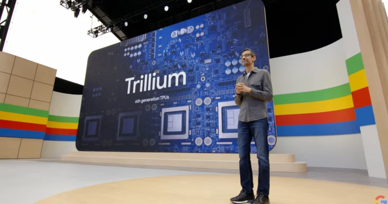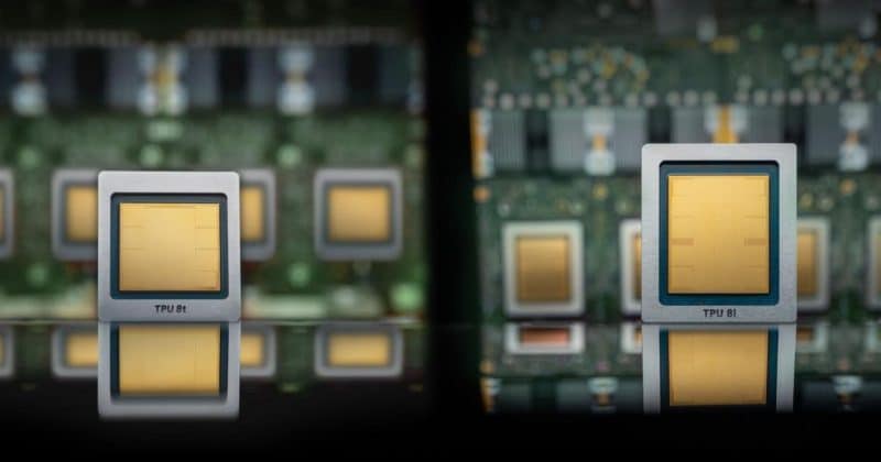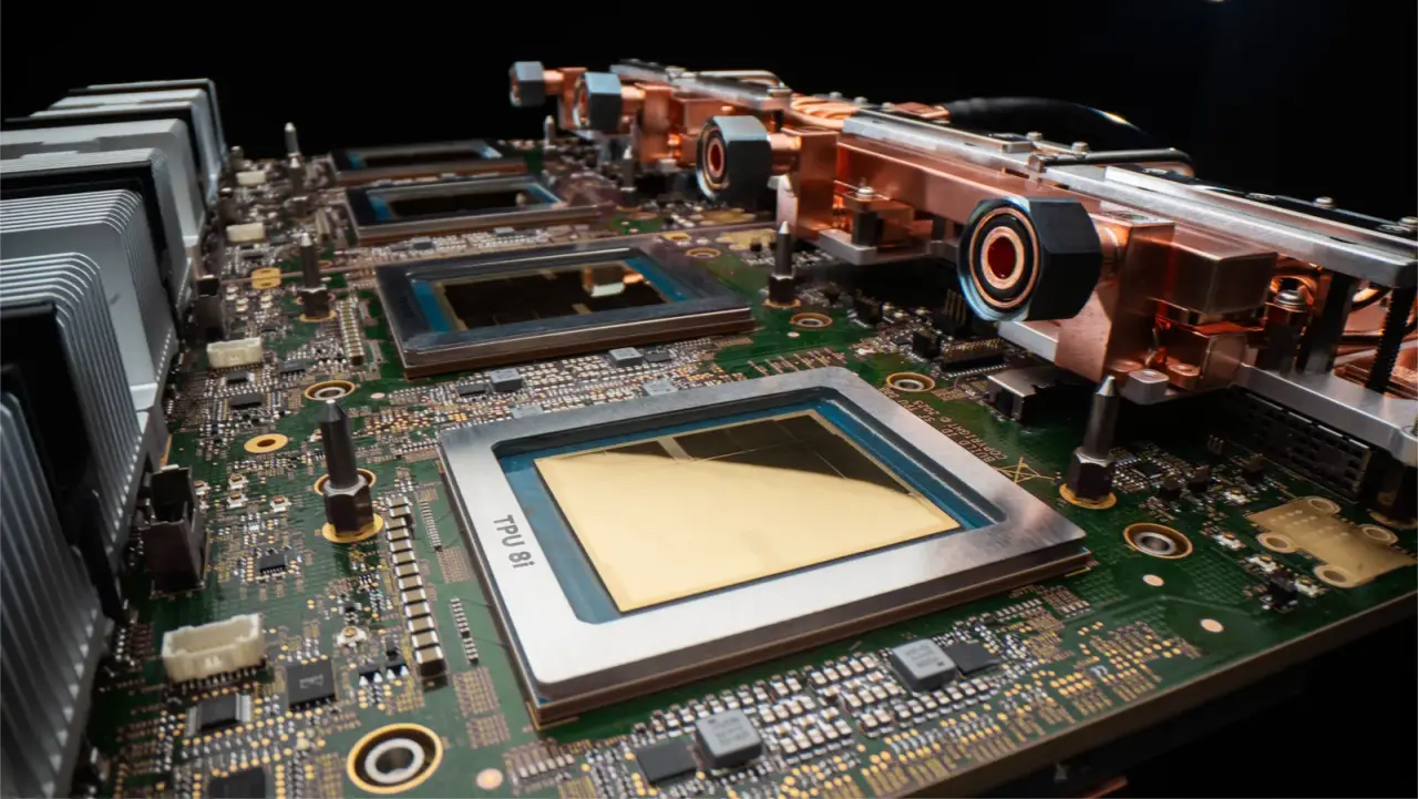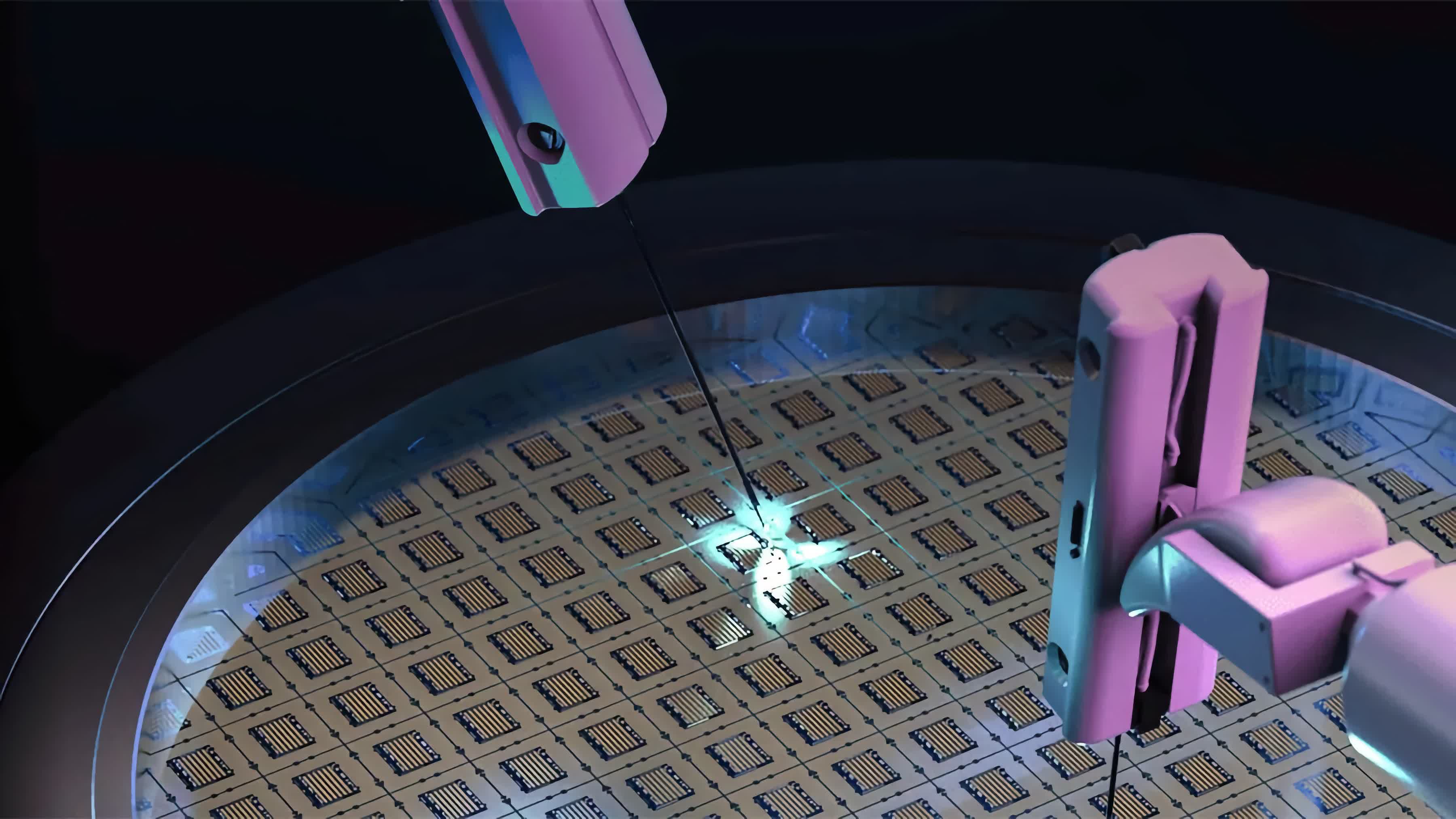
Samsung Electronics is reportedly in consideration to take on back-end design work for Google’s next-generation 2nm Tensor Processing Unit. If the deal materializes, it would represent a notable shift in how Google sources the engineering behind its custom AI chips, and a meaningful win for Samsung’s foundry ambitions.
Back-end design is the stage where a chip’s logical blueprint gets translated into the actual physical layout that can be manufactured. It’s painstaking, precision-critical work, and the fact that Google is looking outside its own walls for it tells you something about the complexity of building at the 2nm process node.
Why 2nm matters, and why Samsung wants in
The 2nm process node is the bleeding edge of semiconductor manufacturing. Smaller transistors mean more computing power crammed into less space, with better energy efficiency. For AI workloads, where TPUs chew through enormous datasets inside Google’s data centers, every incremental improvement in power and performance translates directly into lower operating costs and faster model training.
Google has been designing and deploying TPUs since 2016, initially to accelerate machine learning tasks across its cloud infrastructure.