Tensordyne targets AI inference market with logarithmic math and Juniper-derived rack architecture
The race to serve AI inference faster and cheaper is exposing the hard limits of conventional chip architecture. As demand for real-time AI responses accelerates, the industry’s standard response — stacking more high-bandwidth memory onto power-hungry silicon — is running into a wall, and logarithmic math may be the foundational rethink that breaks through it.
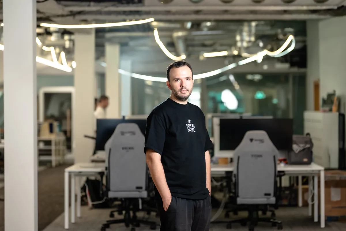
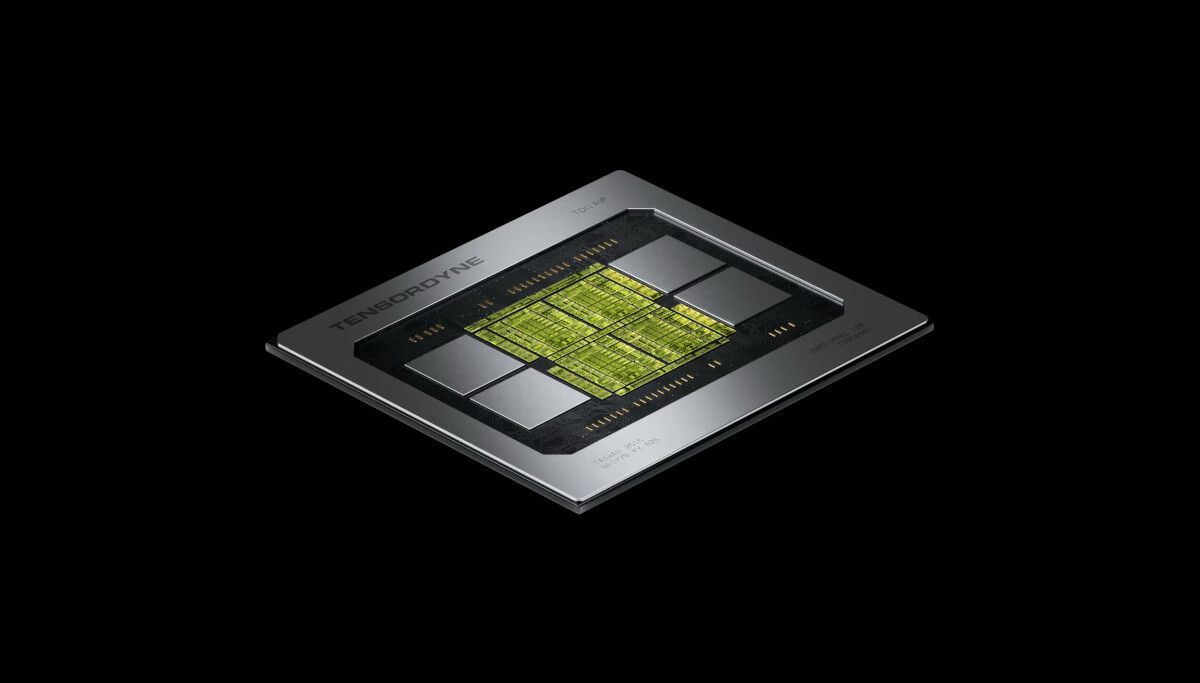
Fresh out of stealth and with its first chip now in production at Taiwan Semiconductor Manufacturing Co., Ltd., Tensordyne Inc. is positioning itself to challenge the AI inference market by rearchitecting the math inside the silicon — not just the chip itself — according to Gilles Backhus (pictured), co-founder of Tensordyne.
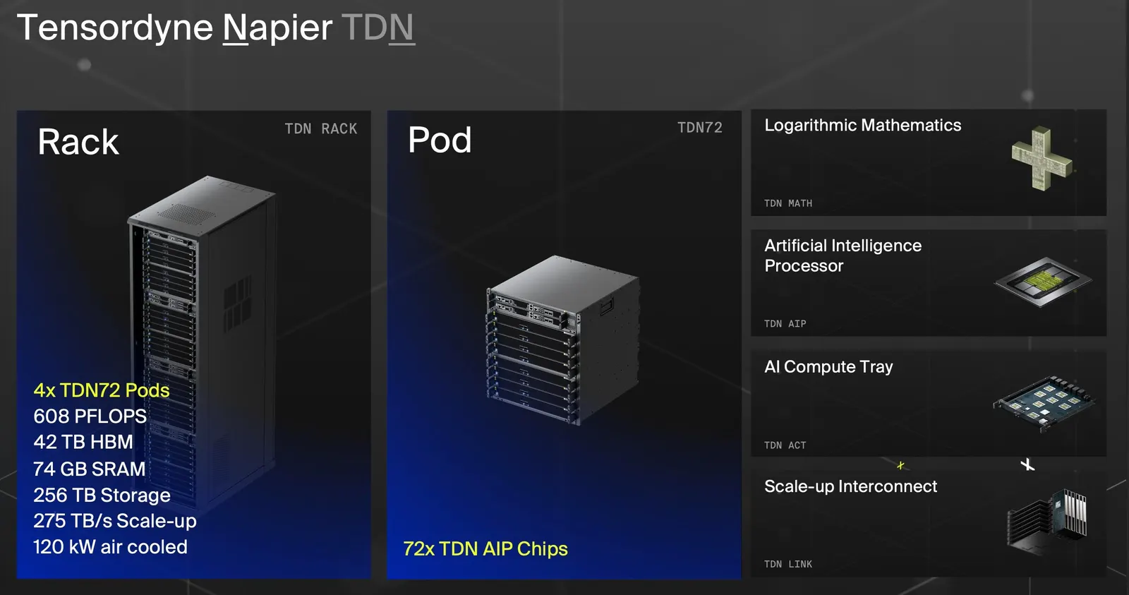
“Our logarithmic math — it’s completely under the hood,” Backhus said. “From a user point of view, from an SDK point of view, you don’t even notice it. It just looks like normal floating-point math. It’s just that the engine under the hood is more efficient.”
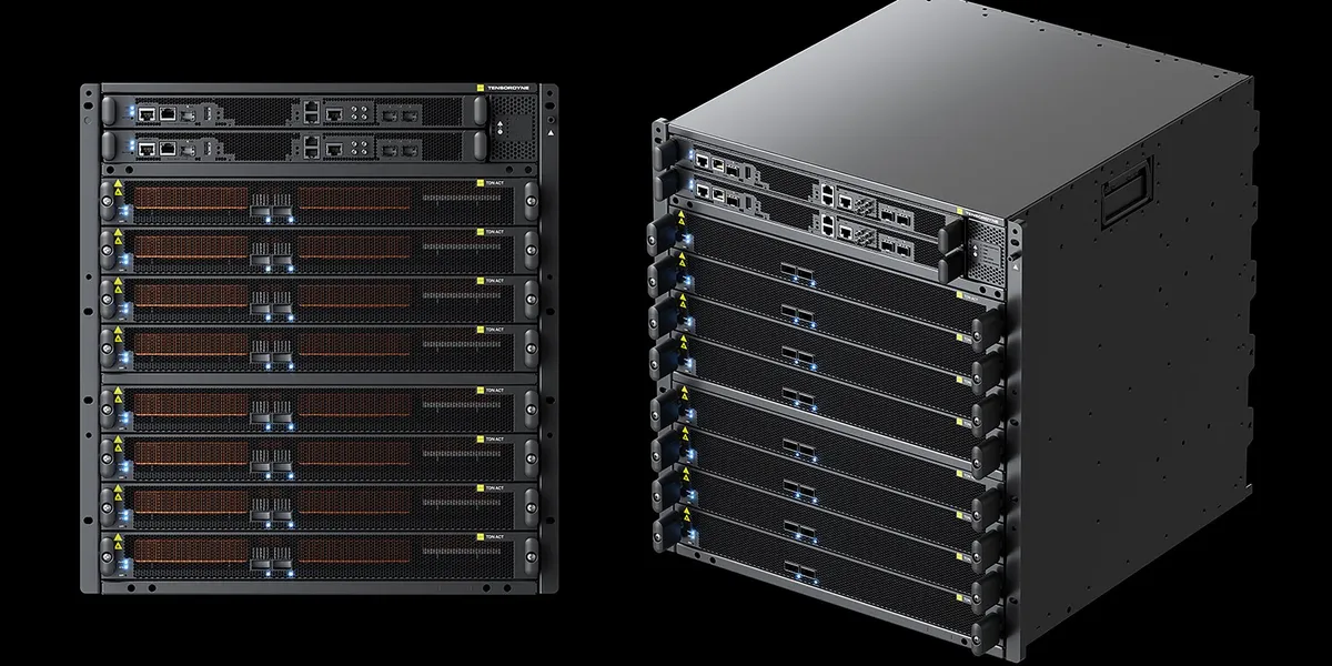
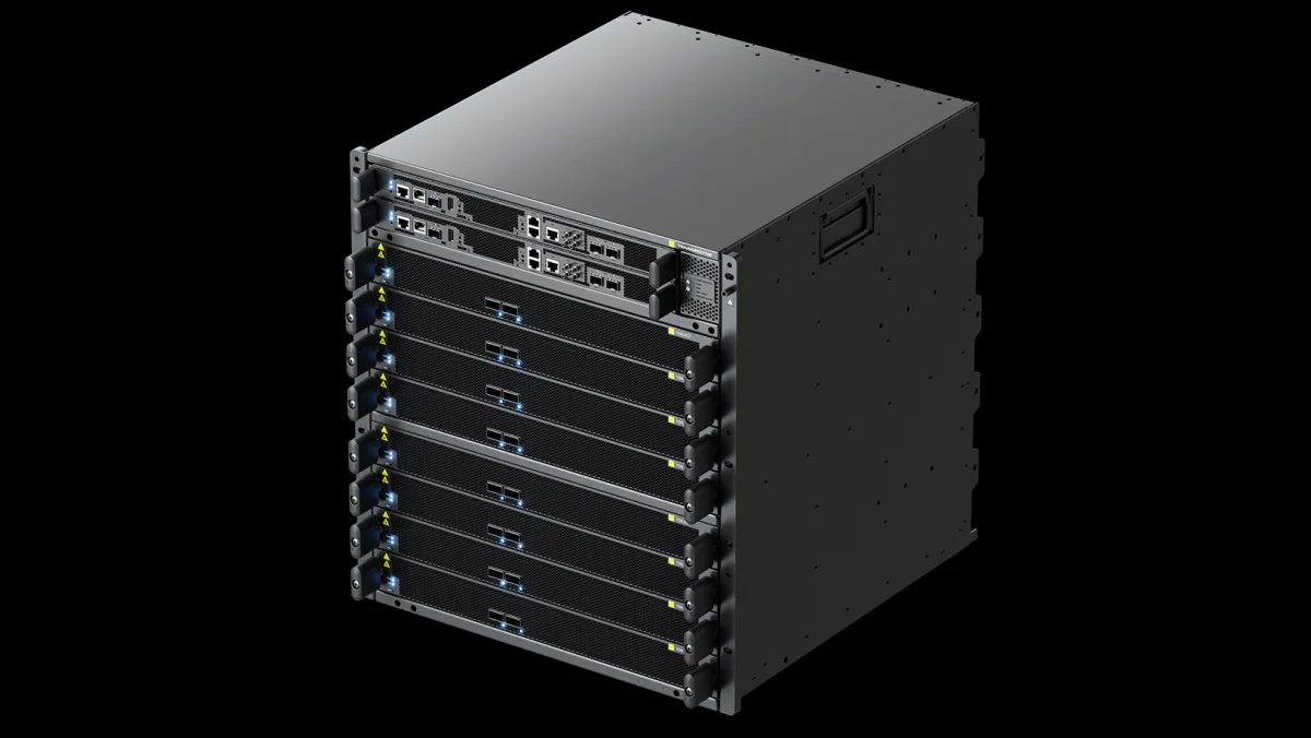
Backhus spoke with theCUBE’s John Furrier at the RAISE Summit, during an exclusive broadcast on theCUBE, SiliconANGLE Media’s livestreaming studio. They discussed how Tensordyne’s cross-continental co-design model, logarithmic math innovation and Juniper Networks-derived rack architecture are positioning the company as a direct challenger to Nvidia Corp. in the AI inference infrastructure market. (* Disclosure below.)