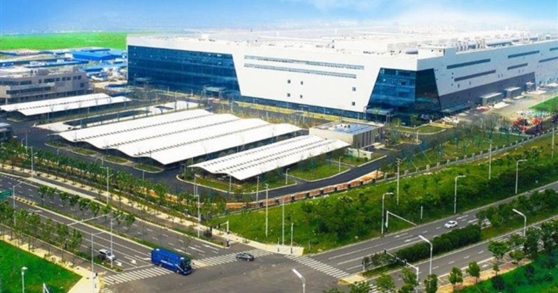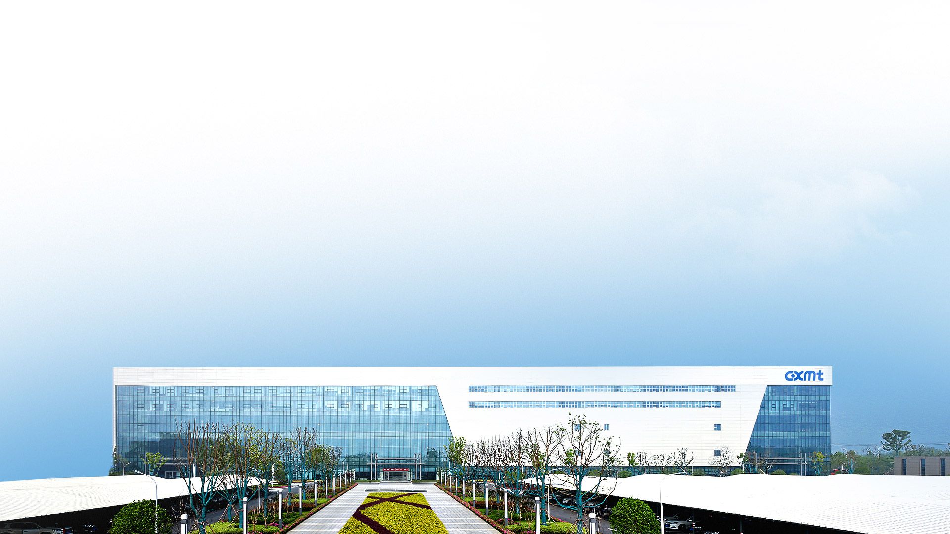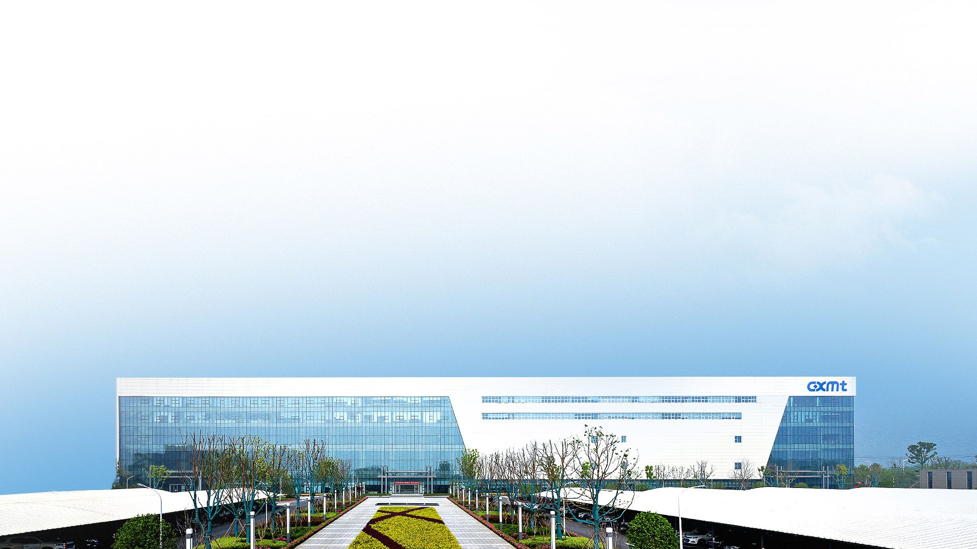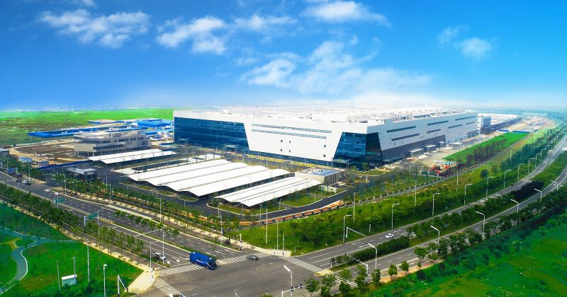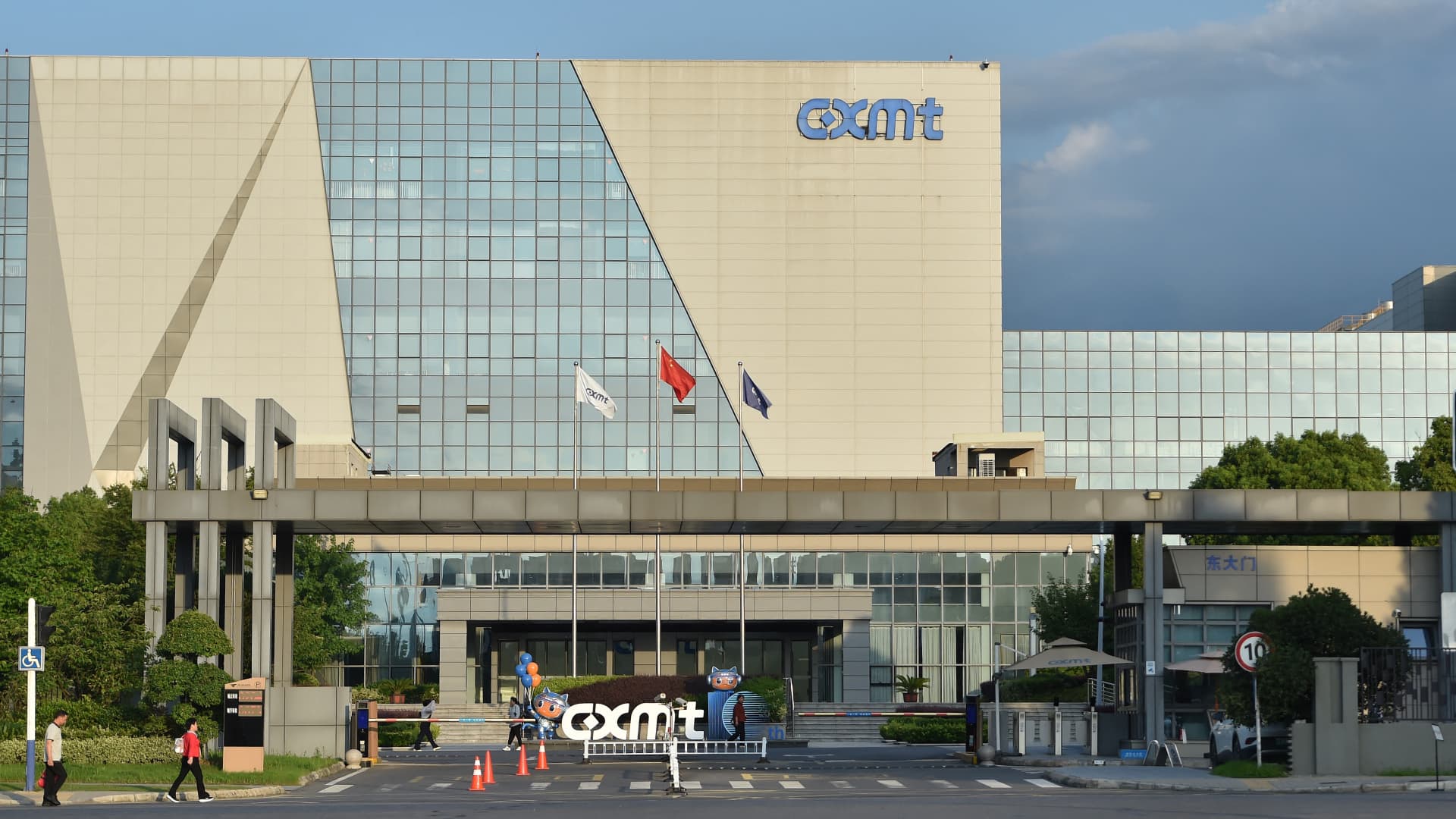
ChangXin Memory Technologies, China’s leading DRAM manufacturer, is testing a pilot production line for bonded DRAM at its Hefei facility. The technology uses wafer-to-wafer hybrid bonding to build high-density memory chips without relying on extreme ultraviolet lithography, the single most expensive and export-restricted tool in the semiconductor supply chain.
What bonded DRAM actually is and why it matters
Traditional DRAM manufacturing puts memory cell arrays and peripheral circuitry on the same piece of silicon. As chips shrink, this gets harder, and eventually you need EUV lithography to print features small enough to keep pace. EUV machines, made exclusively by the Dutch firm ASML, are subject to strict export controls that effectively block Chinese chipmakers from acquiring them.
Bonded DRAM takes a different approach. It separates the memory cell arrays from the peripheral circuits, fabricates them on different wafers, and then bonds them together. The result is high-density, high-performance DRAM that can theoretically be produced on older lithography equipment.
South Korean media first reported CXMT’s bonded DRAM pilot line around July 5, 2026. The timing is notable because Samsung is pursuing a similar approach with its own B1b project, and SK Hynix has also been exploring bonded architectures. Korean analysts have noted that CXMT could potentially gain a technological edge if it reaches commercialization first.