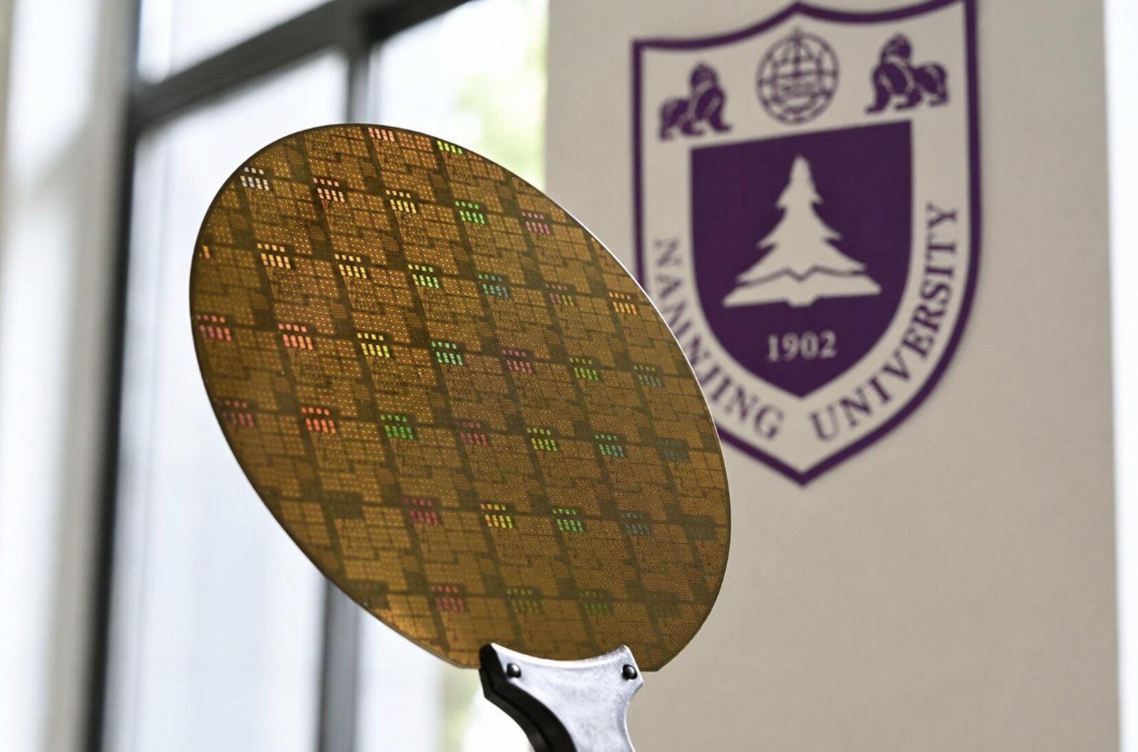
A tandem neural network capable of inferring key physical parameters of semiconductor materials from simple transistor measurements has been developed, as reported by researchers from the Institute of Science, Tokyo. While conventional approaches for this type of analysis require hours or even days, the proposed system produces results in under 1 millisecond with near-perfect accuracy.
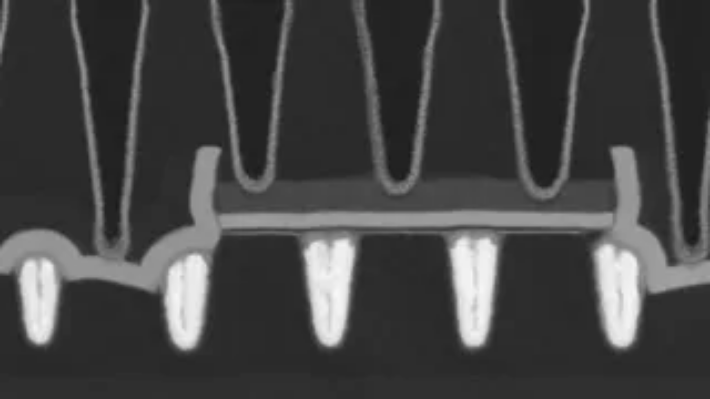
Modern electronics rely heavily on semiconductor devices, whose performance is shaped by material properties like defect density and charge transport characteristics. Even though it's relatively easy today for engineers to measure how a transistor behaves, determining the underlying material properties responsible for that behavior remains far more difficult.
This type of "inverse" analysis is essential for developing better electronics and improving manufacturing processes, and thus finding efficient ways of probing semiconductor materials is becoming increasingly important.
One of the main difficulties when dealing with such inverse problems is related to what scientists call "multivaluedness." Simply put, because different combinations of material properties can produce nearly identical transistor characteristics, it is quite challenging to work backward—that is, identify the physical properties of a semiconductor material based solely on device performance measurements.