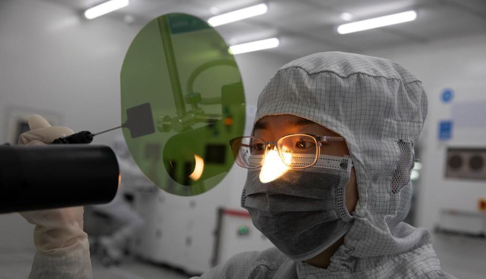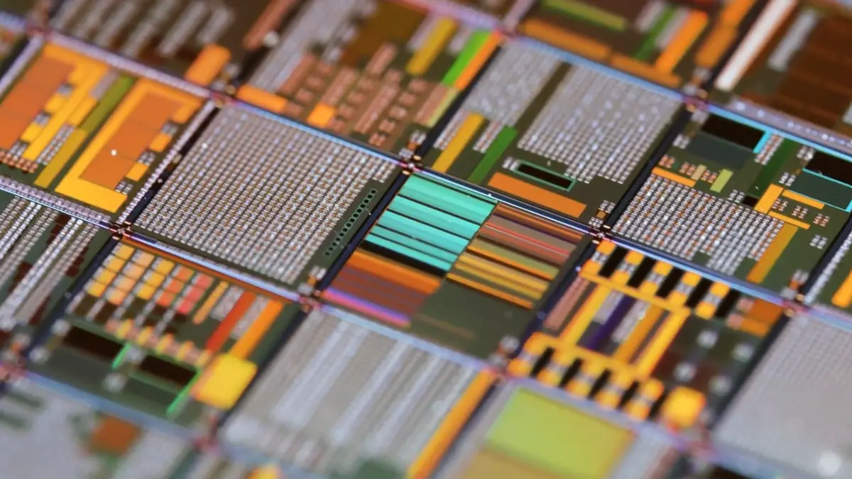
In the heart of every modern electronic device lies a silicon chip, built through a manufacturing process so precise that even a microscopic defect can determine success or failure. As semiconductor devices grow more complex, reliably detecting and classifying defects has become a critical bottleneck.
Historically, chipmakers have relied on convolutional neural networks (CNNs) to automate defect classification (ADC). But as manufacturing scales and diversifies, CNN-based approaches are hitting their limits, requiring large labeled datasets, frequent retraining, and still struggling to generalize across new defect types.
In this post, we show how generative AI-powered ADC can overcome these challenges.
The workflows below leverage NVIDIA Metropolis vision language models (VLMs), vision foundation models (VFMs), and the NVIDIA TAO fine-tuning toolkit to modernize defect classification. We outline the limitations of traditional CNN-based systems, detail how VLMs and VFMs address them, and highlight specific approaches and manufacturing challenges they help solve.
The limits of CNNs in semiconductor defect classification