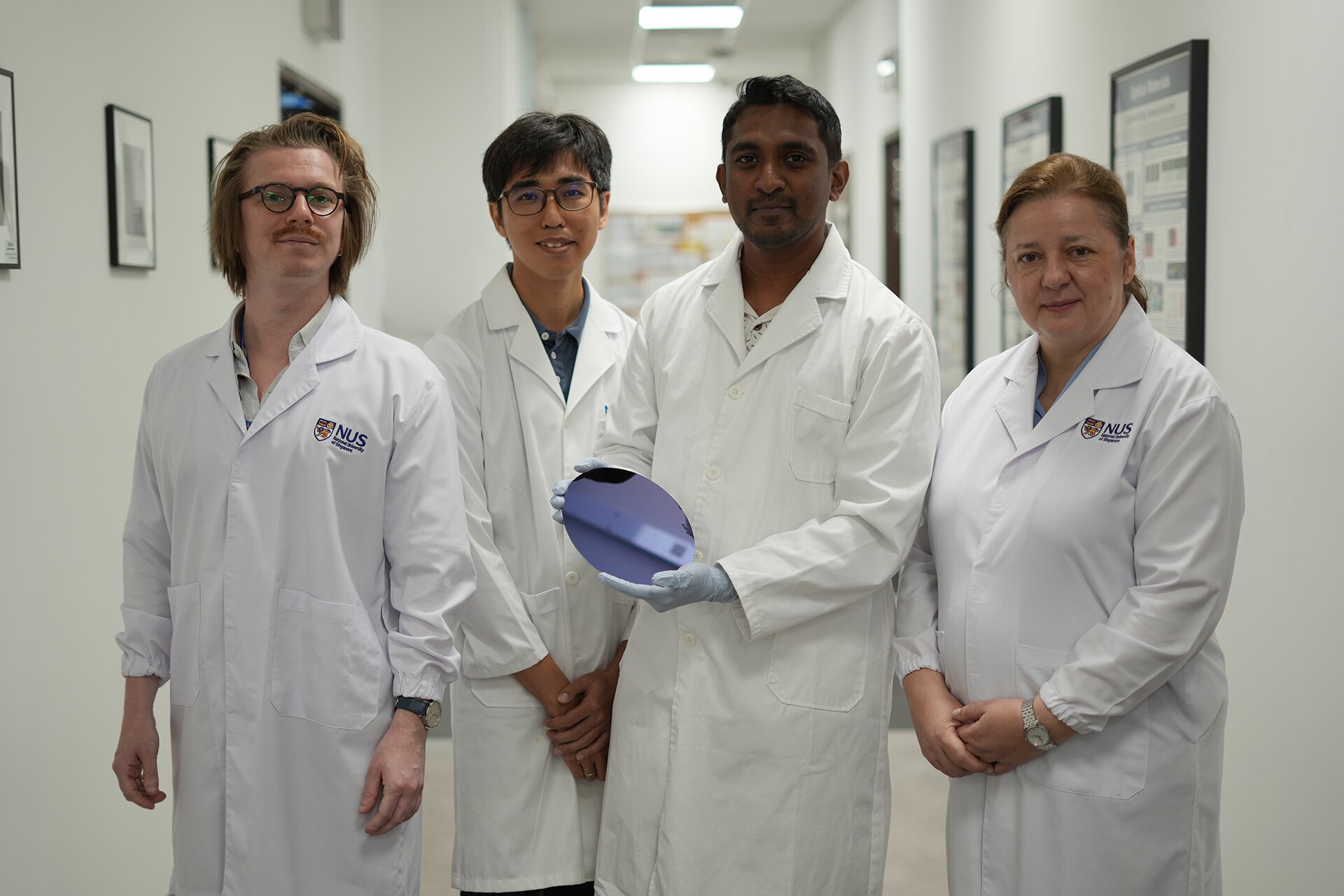
From right: Members of the research team from the Department of Materials Science and Engineering, Prof Silvija Gradečak, Dr. M Juvaid, Dr. Chung Jing-Yang, and Dr. Hippolyte Astier. Credit: College of Design and Engineering, NUS
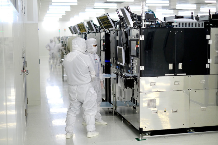
The global semiconductor market is approaching US$1 trillion in annual sales, driven by growing demand for faster computers, smarter AI systems and more powerful electronic devices. Singapore, which produces one in 10 of the world's chips, has a direct stake in sustaining that trajectory.
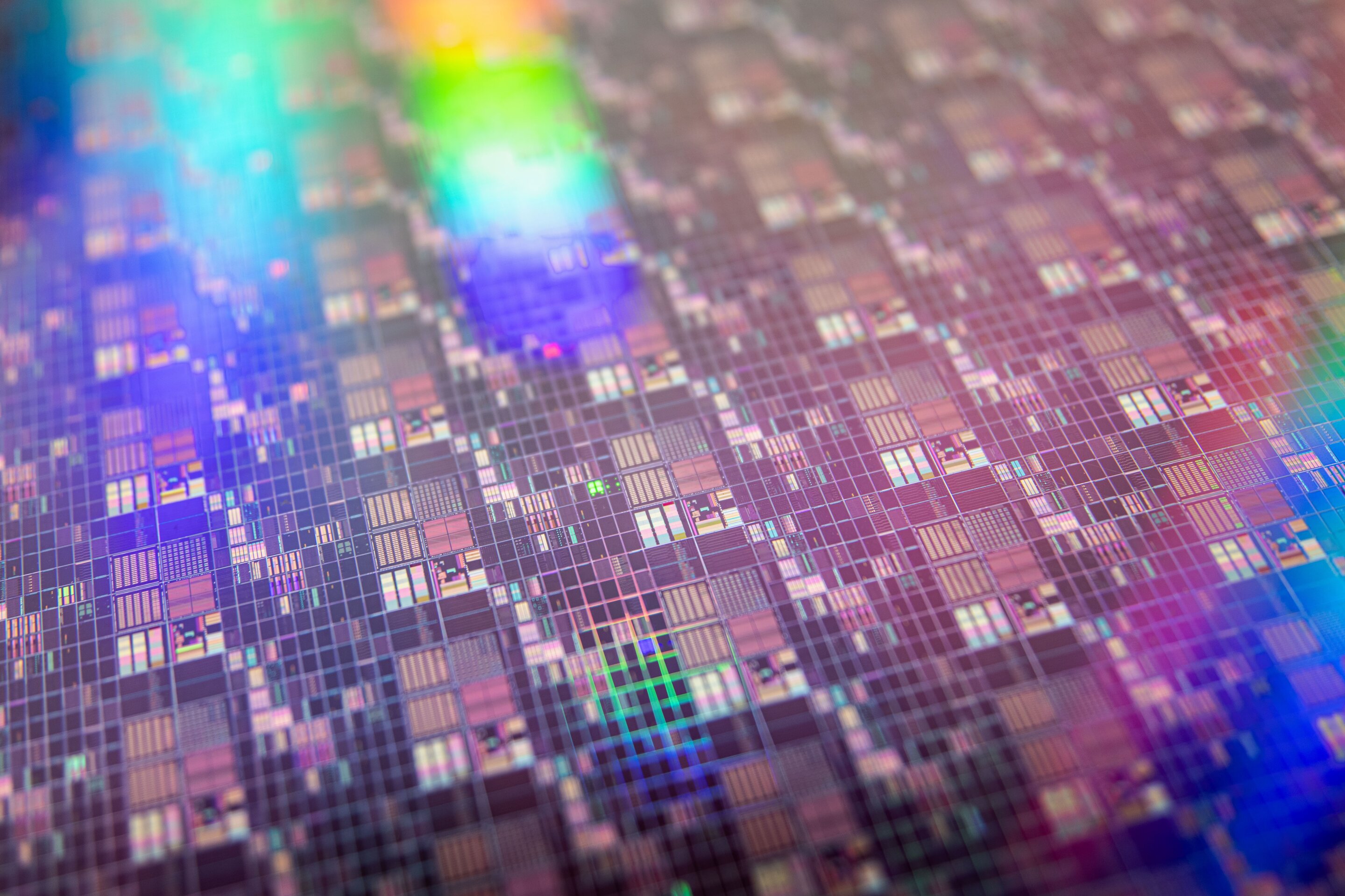
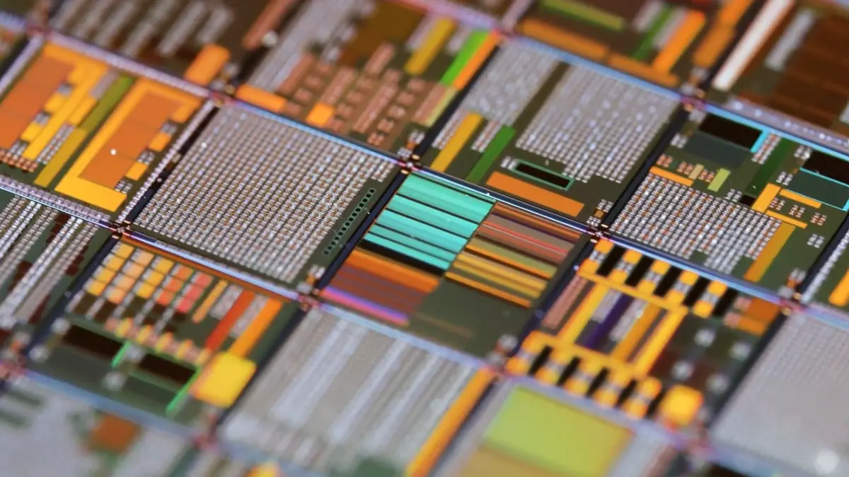
For decades, advances in chip performance have relied on shrinking transistor size, pushing semiconductor technology ever closer to its physical limits. But a bottleneck is emerging at one of the most fundamental levels of chip architecture: the tiny wiring inside computer chips.
While the copper wires connecting transistors are becoming smaller with each new generation, the protective layers around them cannot shrink as easily, making it harder to improve chip speed, efficiency and reliability.
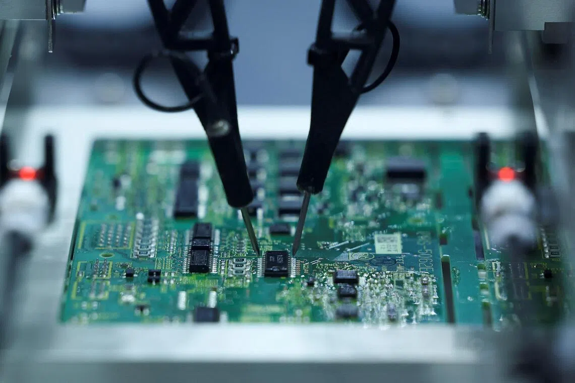
Copper wires inside chips need two protective coatings: a barrier to stop copper atoms from migrating into surrounding materials, which can cause short circuits and chip failure, and a liner to help copper adhere and form smooth, reliable connections.