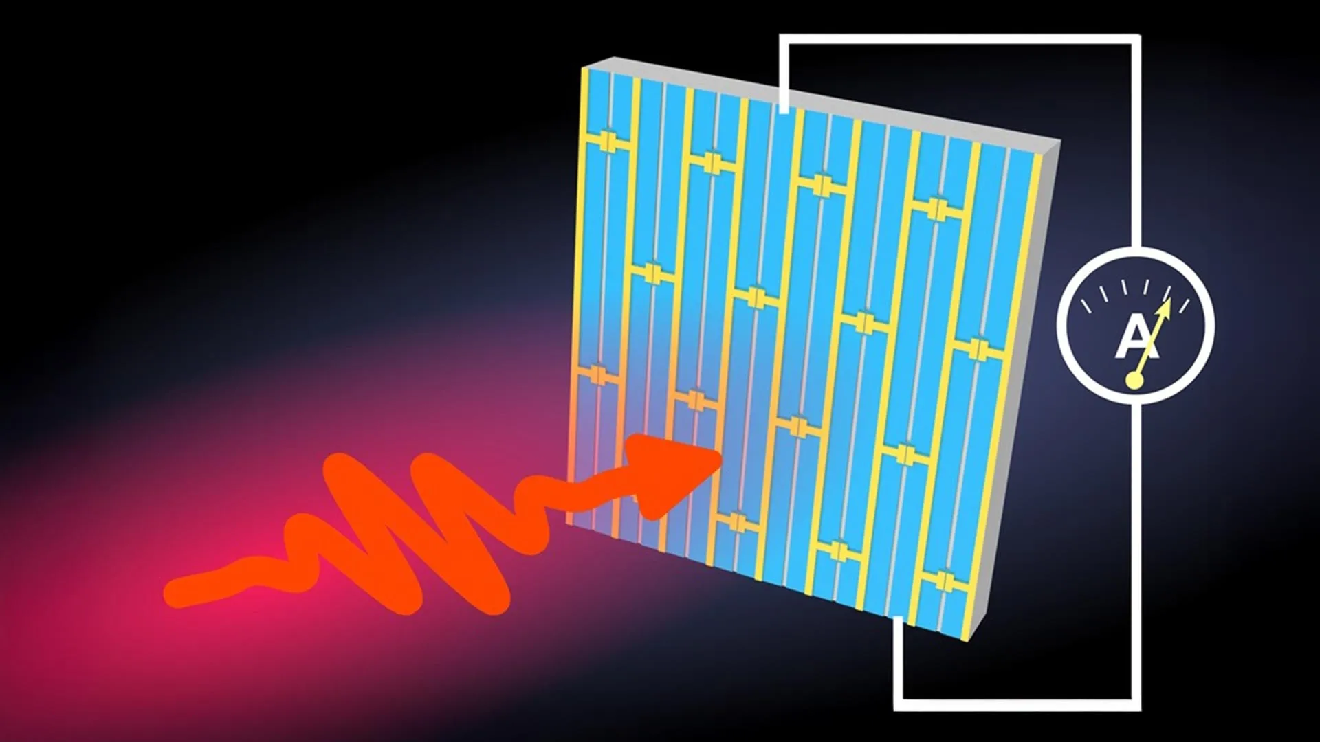
High-frequency waves classified as terahertz occupy a relatively underused region of the electromagnetic spectrum between infrared light and microwaves. Researchers have long recognized its unique potential for applications including ultrafast wireless communication, security screening, remote sensing and medical imaging.
As technologies push toward higher operating frequencies and data rates, photonics-based terahertz systems, which use light at superspeed to generate and process terahertz signals, have emerged as a promising alternative to conventional electronic technologies because of their superior bandwidth and power efficiency. However, today’s terahertz optoelectronic systems, which are electronic systems that control light, remain bulky, complex and difficult to scale for widespread use. They typically rely on multiple separate components — including lasers, amplifiers, modulators, sources and detectors — that must be individually made, aligned and interconnected, limiting use outside specialized laboratory settings.
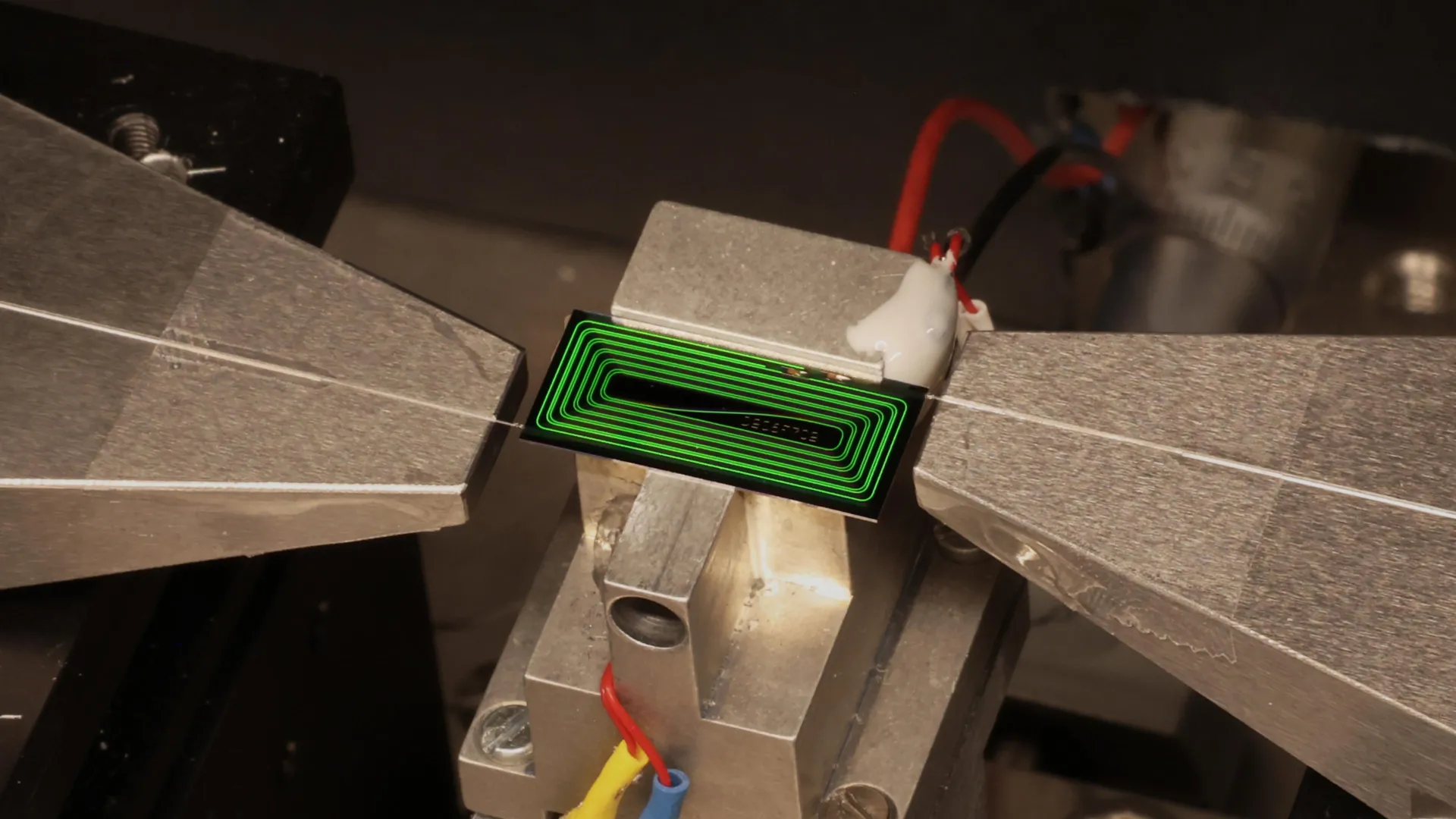
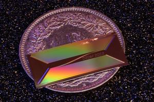
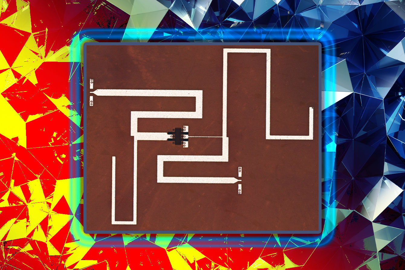
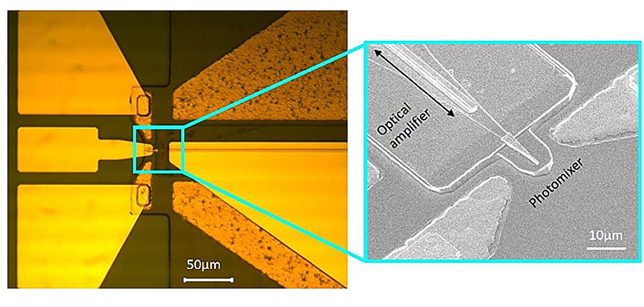
Now, a UCLA-led research team has demonstrated a way to integrate these functions onto a single semiconductor chip compatible with modern photonic technologies. The breakthrough, published in Nature Communications, paves the way for compact, scalable terahertz systems for next-generation communication, imaging and sensing applications.