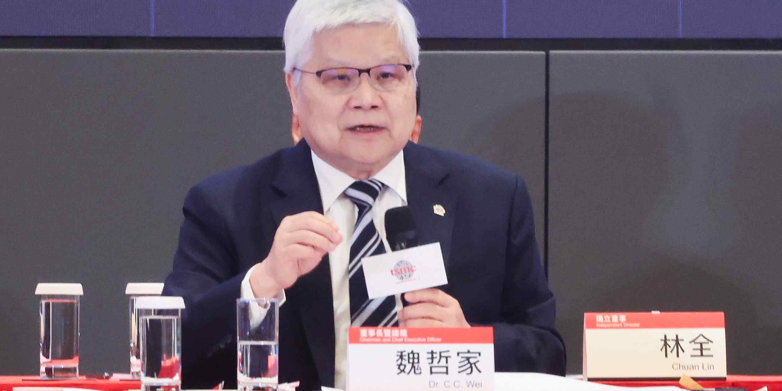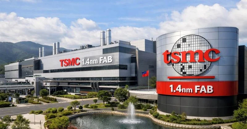
The semiconductor packaging war just got a new chapter. At TSMC’s North America Technology Symposium on April 22, 2026, Deputy Co-COO Kevin Zhang made it clear that the world’s largest contract chipmaker isn’t losing sleep over Intel’s advances in advanced packaging, even as major hyperscalers start exploring alternatives.
The confident posture comes at an interesting moment. Google has reportedly adopted Intel’s Embedded Multi-Die Interconnect Bridge (EMIB) technology for at least one project, choosing it over TSMC’s offerings due to advantages in reticle size. Amazon is also reportedly showing increased interest in Intel’s EMIB technology.
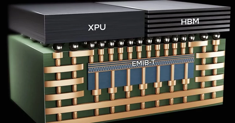
The packaging technology battle, explained
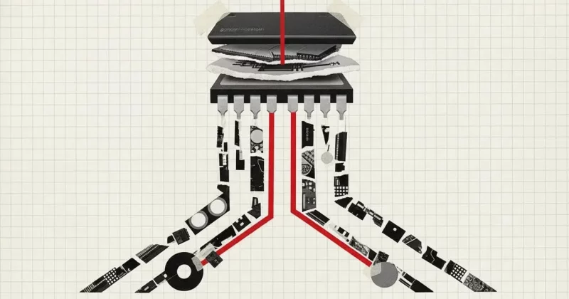
TSMC has built its packaging empire around a family of technologies called CoWoS, short for Chip-on-Wafer-on-Substrate. The CoWoS family includes several variants, CoWoS-S, CoWoS-R, and CoWoS-L, each optimized for different use cases. These technologies are the backbone of high-volume AI chip production, including NVIDIA’s GPUs that power the current AI infrastructure boom.
Intel’s counter-move is EMIB, which embeds small silicon bridges directly into organic substrates. It’s a 2.5D packaging solution that competes directly with CoWoS.