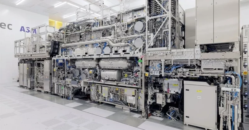
TSMC Chairman C.C. Wei confirmed at the company’s annual shareholder meeting on June 4 that the foundry giant has purchased ASML’s High-NA EUV lithography systems, but strictly for research and development. The message was clear: these tools are not ready for the production floor, and the price tag is the main reason why.
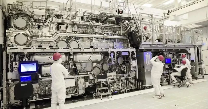
Each High-NA EUV system costs approximately $400 million. That is roughly double the price of previous-generation EUV tools, which were already among the most expensive pieces of industrial equipment ever manufactured.
The $400 million question
High-NA EUV represents the next frontier in semiconductor lithography, the process of etching impossibly small circuit patterns onto silicon wafers. “NA” stands for numerical aperture, which determines how fine those patterns can be. A higher numerical aperture means smaller, more densely packed transistors, which means faster and more efficient chips.
TSMC’s R&D teams are now tasked with figuring out how to make these systems economically viable before they ever see a production wafer. Wei emphasized that the company is committed to enhancing cost-effectiveness ahead of any potential volume manufacturing.