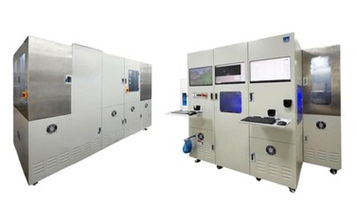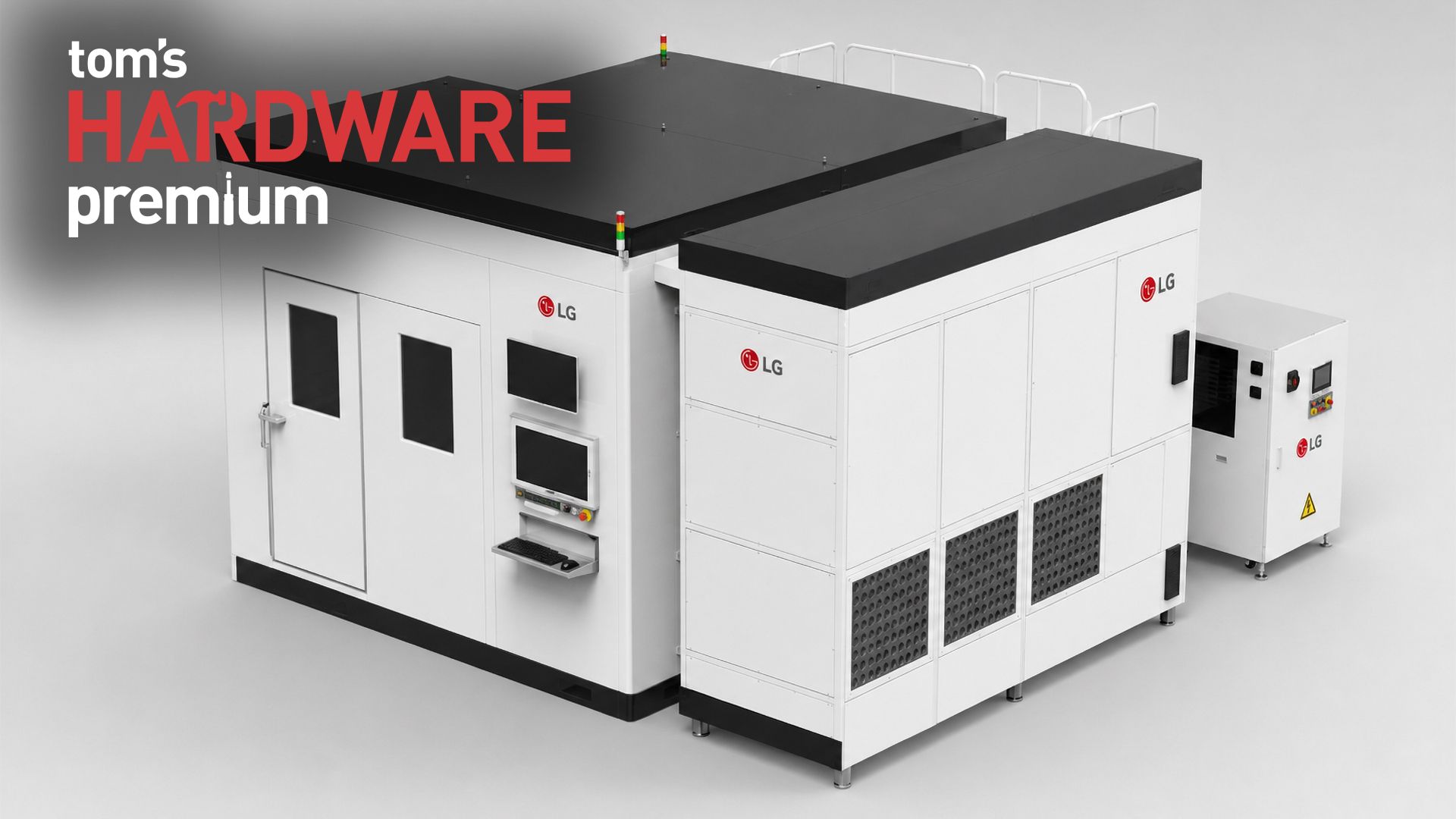
As advanced packaging technologies like EMIB and CoWoS become yet another battlefield in the semiconductor industry, outsourced semiconductor assembly and test (OSAT) companies are trying new tools in a bid to offer services that others do not. This week, LG Electronics Production Technology Institute (PRI) signed a contract with an OSAT to supply it with a maskless laser direct imaging (LDI) lithography tool that can be used to build metal-interconnect patterns in semiconductor packaging, potentially with higher yields than currently available tools, reports ETNews.LG-PRI's Laser Direct Imaging (LDI) system is a maskless lithography machine designed to pattern fine metal interconnects for advanced semiconductor packaging. While the company has developed various versions of the machine, its highest-resolution version can produce 1.5-µm line-and-space (L/S) patterns, which should be fine to 'print' wiring pitches of about 3 µm. The production equipment uses a 405-nm laser-diode light source and can process substrates as large as 600 × 600 mm, according to various media reports.
LG enters chip packaging arena with Laser Direct Imaging machine, as TSMC's CoWoS remains constrained — maskless machine is designed to pattern fine interconnects, trading resolution for higher throughput
LG rolls-out laser direct imaging lithography machine for chip packaging and high-density PCBs.
TL;DRAI
LG-PRI unveiled a maskless LDI tool achieving 1.5-µm interconnect resolution for advanced packaging, addressing TSMC CoWoS capacity constraints. Signals shift toward OSAT diversification and potential pricing pressure on TSMC's packaging services amid rising demand for advanced assembly capacity.
160 words~1 min read