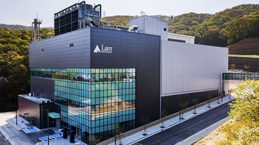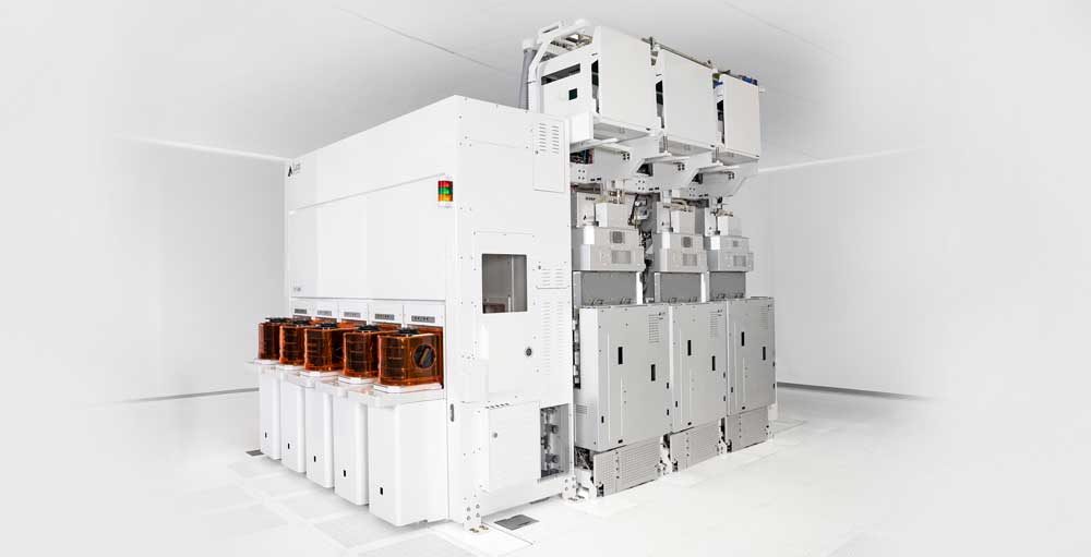
InnovationgettyI attended LAM Research’s Future of AI and Semiconductors Event last week. LAM manufactures advanced semiconductor etching, including the deep etching required for creating 3D NAND memory cells, and plating solutions and has an active program to support advanced packaging and heterogeneous integration. The event featured investment pitch presentations from 10 startup participants from all over the world, selected from 180 applicants, with a total prize for the participants of $1M, see below.LAM Research Capital Venture Pitch ParticipantsTom CoughlinThe participants were involved in industries such as advanced robotics, generative and physical AI, heterogeneous integration, semiconductor manufacturing, photonics and other topics. One of these other topics including a magnetic memory technology from a Belgian company called Vertical Compute, presented by the company’s CEO and co-founder, Sylvain Dubois. The overall winner of the competition was Diana Mojahed, founder and CEO of Lightfinder. Her company is developing a breakthrough photonics-based metrology solution enabling real-time process control. The runner-up was nsc (New Silicon Corporation), a Singapore-based statup developing optical interconnect technology and heterogeneous integration of III-V semiconductors to CMOS for photonic devices.Vertical Compute is a spin off from imec, the advanced nano-technology development consortium located in Belgium. The company is offering a vertical integrated magnetic memory technology, shown below. Vertical Data Magnetic MemoryTom CoughlinThe bits are stored as patterns of magnetic domains in a vertical magnetic wire and are read using a magnetic tunnel junction device. This approach is somewhat similar to the racetrack memory technology proposed by Stuart Parkin at IBM several years ago. It is integrated into standard semiconductor logic in a back end of line process and is intended to be a 3D chiplet device that reduces the communication path from data to compute from centimeters to 10’s of nanometers, roughly six orders of magnitude reduction. Shorter path length provides better performance and lower energy consumption than conventional DRAM based memories.The performance and expected memory density improvements for this non-volatile memory technology compared to SRAM and DRAM is shown below. The potential of this technology to replace conventional volatile memories for AI applications is very high.Vertical Compute memory versus SRAM and DRAMTom CoughlinLAM also was showing the company’s work to support advanced semiconductor packaging that includes the companies SABRE 3D product family for electrochemical deposition for electroplating of coper and other metals to creating high-density micro-bumps and filling through-silicon via (TSV) structures. Lam also has a VECTOR TEOS 3D for very thick, void-free dielectric gapfill with advanced wafer clamping for dimensional stability, a Syndion product family that provides deep reactive ion etch for high precisions TSV etch and plasma dicing for high yield 3D integration, and its Striker atomic layer deposition (ALD) product.LAM was also displaying panel-level solutions, see below, to support chiplets and advanced packaging solutions. These panels may be made from organic materials, including fiberglass, glass and silicon.300mm Silicon wafer and panels at LAM eventTom CoughlinThis image shows a conventional 300mm silicon wafer besides a couple of panel solutions. These solutions include advanced electrochemical deposition platforms Kallisto and PHOENIX for ultra-line plating and high-throughput processing at panel scale, advancing cost-efficient, large-format advanced packaging manufacturing. LAM Research recently hosted a Capital Venture Competition that included Vertical Compute’s magnetic memory technology and showed the company’s panel solutions for advanced semiconductor packaging.
LAM Research Event Shows Key Chiplet Technologies, Awards Innovators
LAM Research hosted a Capital Venture Competition and showed the company’s panel solutions for advanced semiconductor packaging.
540 words~2 min read