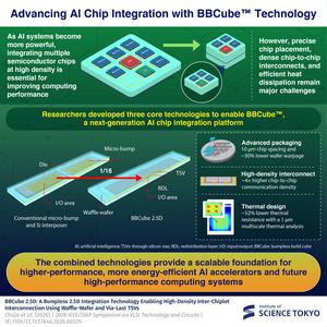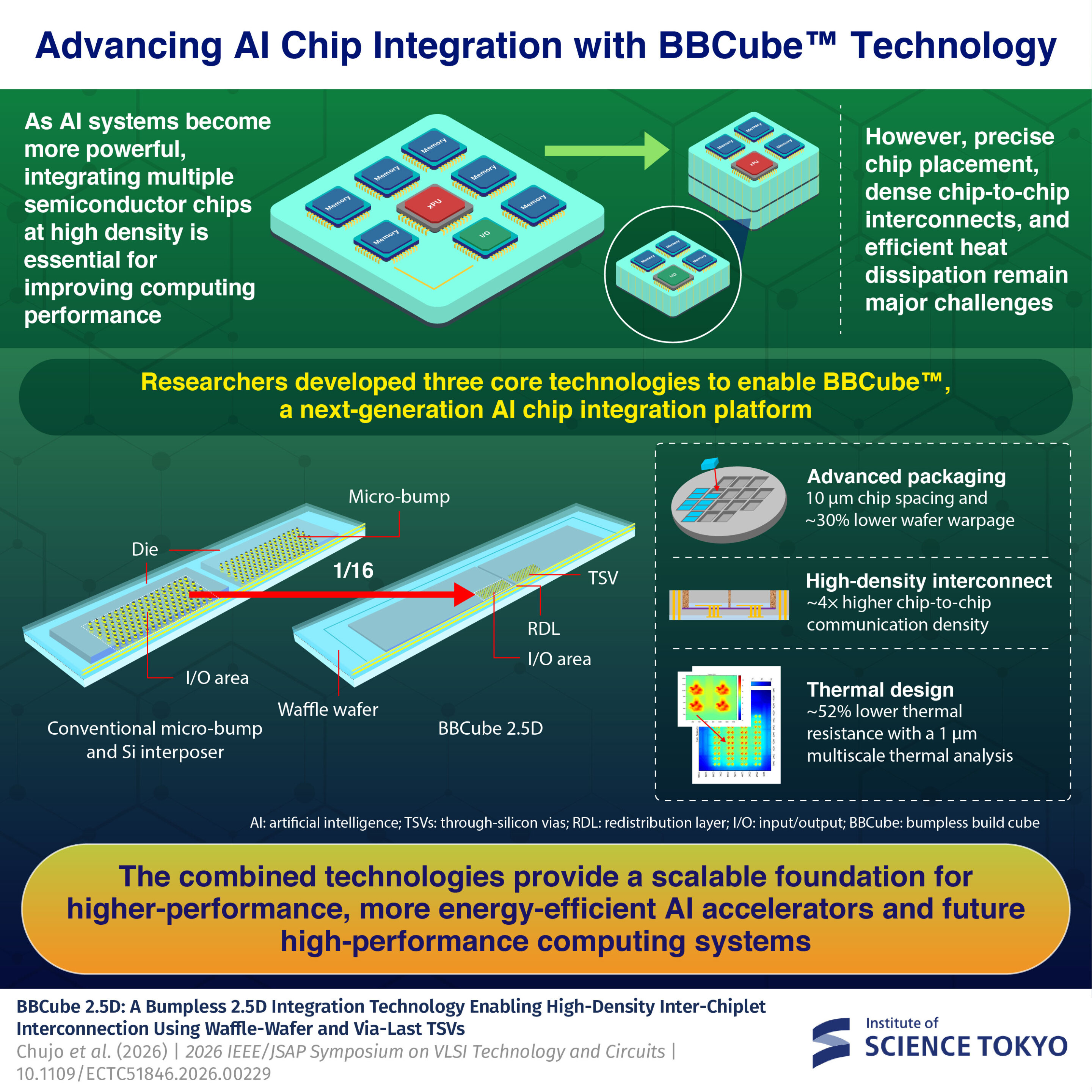
Researchers combine three core strategies to overcome barriers in semiconductor packaging and enable compact, high-performance semiconductor systems. Credit: Institute of Science Tokyo
A new semiconductor integration platform developed at the Institute of Science Tokyo combines advanced chip packaging with high-density interconnects and improved thermal management. This combination of three complementary technologies helps overcome the key challenges in building high-performance artificial intelligence (AI) hardware.
By enabling more precise chip placement, faster communication and efficient cooling, the technology paves the way for more powerful and energy-efficient AI accelerators and high-performance computing systems.
AI is rapidly transforming technologies, creating a growing demand for faster and more powerful computing systems. Meeting these demands requires semiconductor chips that can process massive amounts of data at high speed.
Now, instead of relying on individual chips, manufacturers are focusing on advanced semiconductor packaging, which combines multiple chips into a single package to improve computing performance. However, fitting these chips closer together while ensuring efficient communication and cooling remains challenging.