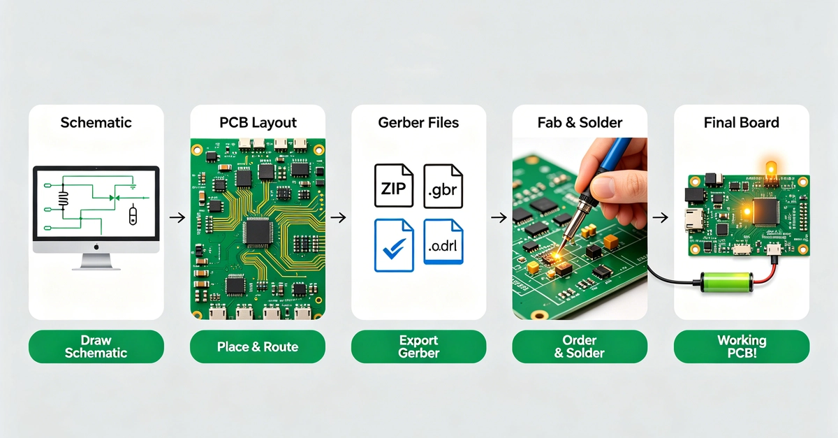
If you've ever designed a board in KiCad, EasyEDA, or Altium, clicked "Export Gerbers," uploaded a zip file to a fab house, and then a couple weeks later a small padded envelope showed up with actual copper-and-fiberglass boards inside — you've probably wondered, at least once, what happens in between. What does a design file actually turn into on a factory floor, and why does it take days instead of minutes?
I went down this rabbit hole recently while debugging why a batch of boards came back with a slightly different impedance than I'd simulated. Understanding the fabrication pipeline turned out to be useful for more than just satisfying curiosity — it changed how I write my design rule checks. Here's the short version, from a developer's point of view rather than a process engineer's.
Your Gerbers are a set of 2D stencils, not a 3D model
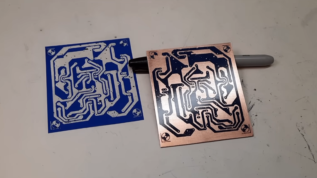
This is the part that took me longest to internalize: a PCB isn't fabricated the way you'd picture a 3D print. There's no printer that magically deposits copper in the right places layer by layer. Instead, each layer of your board starts as full-sheet copper, and the fab removes copper according to your Gerber file for that layer — closer to subtractive manufacturing than additive.