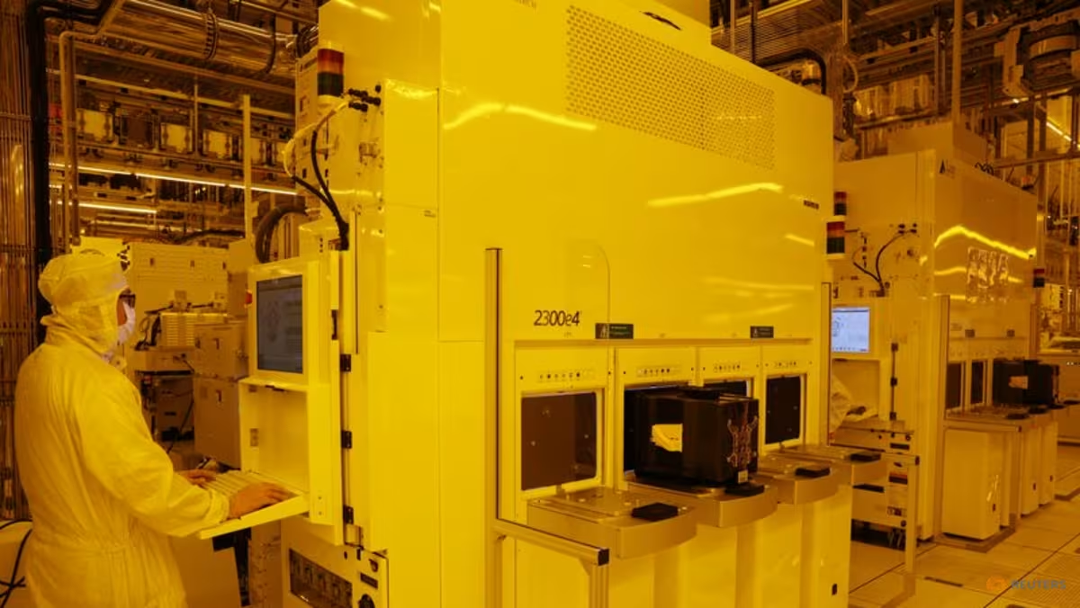
GlobalFoundries just cleared a major engineering milestone. The specialty semiconductor manufacturer announced production readiness for its SLATE wafer-to-wafer bonding technology, a process that enables vertical stacking of transistors and shrinks die sizes by up to 45%.
Volume production is slated to begin in the second half of 2027 at the company’s 300mm fabrication facility in Singapore.
What SLATE actually does
The technology enables homogeneous wafer-to-wafer bonding on GlobalFoundries’ 9SW radio-frequency silicon-on-insulator platform, which launched in 2023. Instead of laying transistors flat across a chip, you stack them like floors in a building.
The result is a die size reduction of up to 45%. This matters for cellular front-end modules, the components that handle signal processing in your phone, including switches, low-noise amplifiers, and antenna tuners.