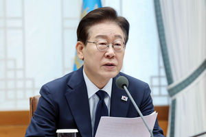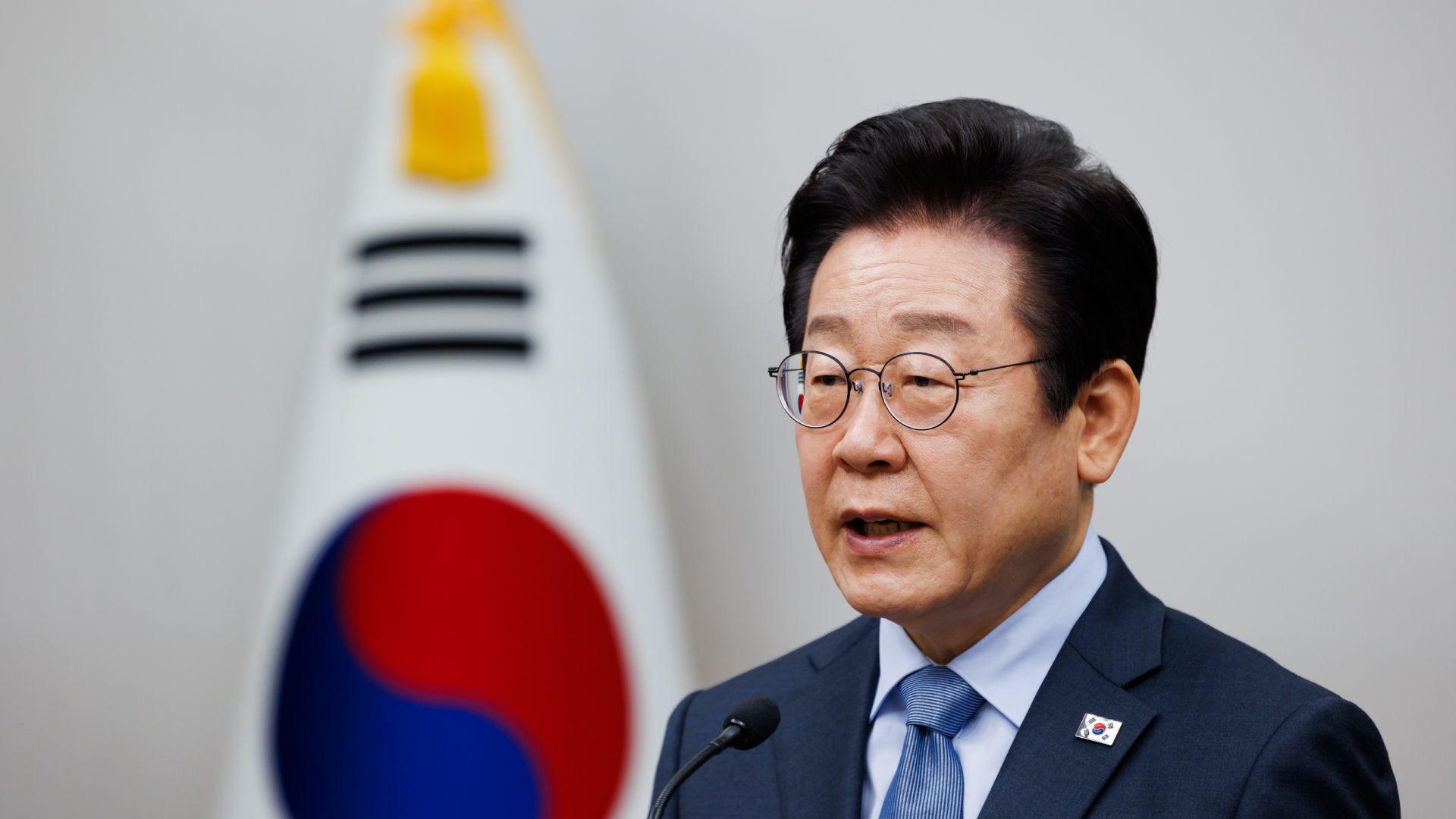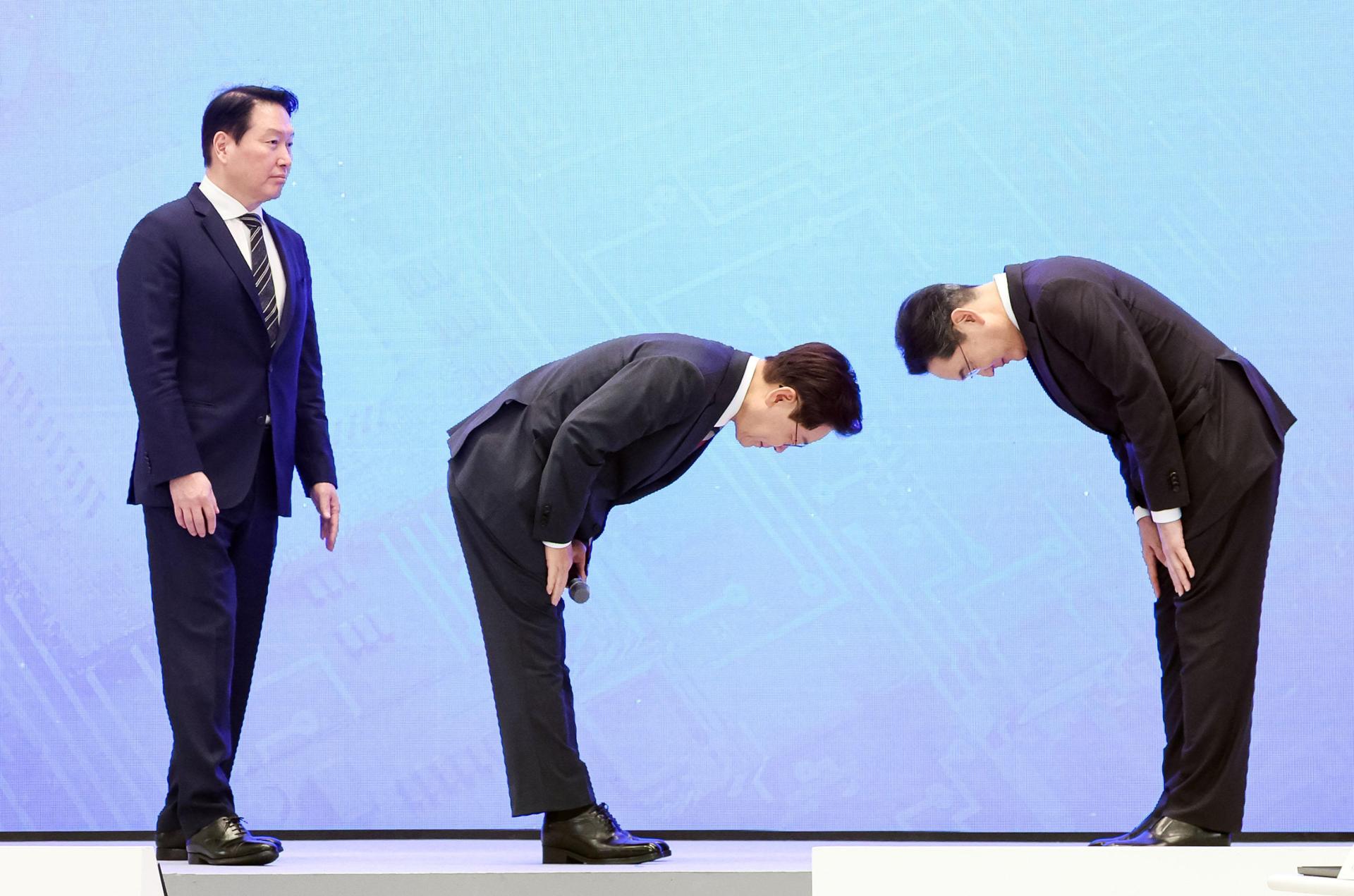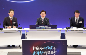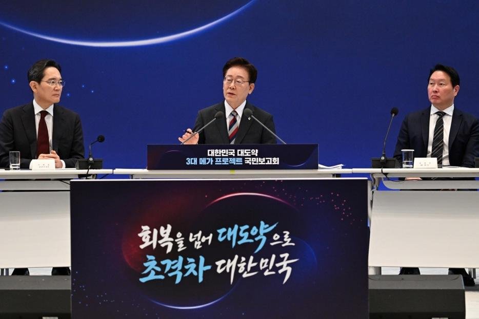
South Korean President Lee Jae Myung (C), Samsung Electronics Chairman Lee Jae-yong (L) and SK Group Chairman Chey Tae-won attend a briefing announcing the government's three mega projects at Yeongbingwan of the Blue House in Seoul on June 29. Photo by Kim Min-hee/EPA/Pool
SEOUL, July 9 (Asia Today) -- This commentary is an outside opinion column written by Young-Han Kim, a professor of economics at Sungkyunkwan University.
On June 29, the presidential office announced the "Three Megaprojects for South Korea's Great Leap Forward" and presented them as the signature policy of President Lee Jae Myung's second year in office.
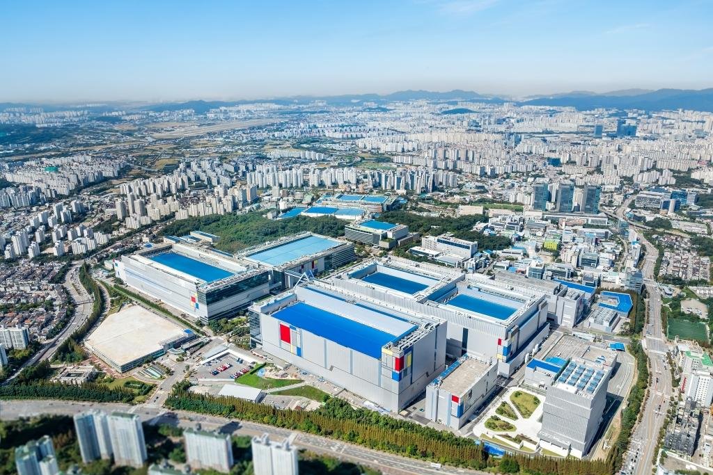
The plan calls for building four ultralarge memory fabs worth 800 trillion won ($522.4 billion) in the Honam region, developing the Chungcheong region into a hub for AI data centers and advanced packaging and nurturing the Yeongnam region as a center for physical AI and supply chains for materials, components and equipment. The government says the plan is designed to mobilize 1,500 trillion won ($979.6 billion) in private investment.
At a public-private inspection meeting Monday, the former Gwangju military airport site was confirmed as the location for the Honam semiconductor cluster. The president said "only speed matters," ordered a shortened environmental impact assessment period and instructed officials to proceed with negotiated land purchases and compulsory expropriation procedures at the same time. He also said the presidential office would create a dedicated body to oversee the project directly. In response to opposition criticism, he said, "Even if you cannot cooperate, do not interfere."