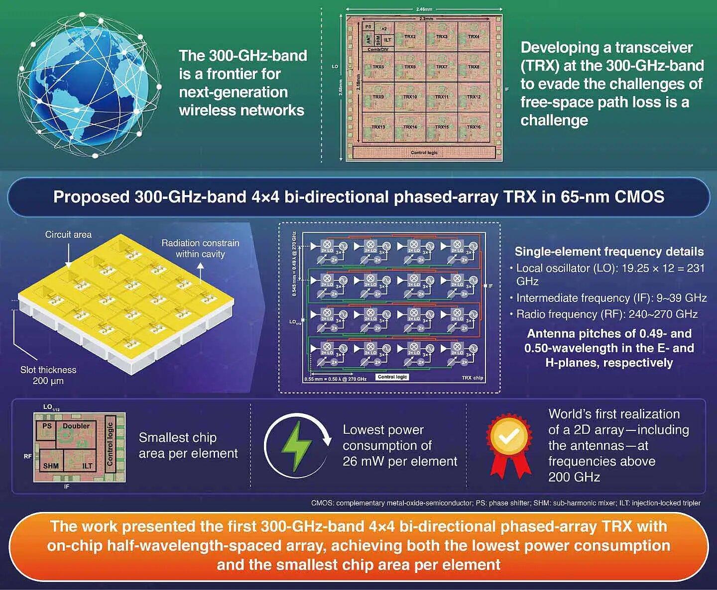
Modern wireless communication systems prefer higher frequencies to meet the growing demand for faster data transfer. The 300-GHz band, which lies near the lower end of the terahertz range, is a promising candidate for future sixth-generation (6G) wireless systems because it can support very high data rates and minimize atmospheric attenuation. However, using such high frequencies comes with major engineering challenges. Radio waves in this range suffer from severe free space path loss (FSPL), making signal transmission challenging over practical distances.
Phased-array transceivers, which combine multiple antenna elements and electronically control their signal phases to steer a radio beam, can help mitigate this limitation. This beam steering can direct energy toward a desired receiver and help recover the link budget. But building compact, low-power phased arrays at around 300 GHz is extremely difficult, especially when the antennas and bidirectional transmit-receive circuitry must fit on the same chip with half-wavelength spacing between the elements.
An all-CMOS terahertz array
A research team led by Professor Kenichi Okada of the Department of Electrical and Electronic Engineering, School of Engineering, Institute of Science Tokyo (Science Tokyo), Japan, has successfully realized a two-dimensional phased-array transceiver capable of wireless communication in the terahertz band, entirely in complementary metal-oxide-semiconductor (CMOS) integrated-circuit technology, including the antennas and bidirectional transmit/receive circuitry. The study, which was presented at the 2026 IEEE/JSAP Symposium on VLSI Technology and Circuits, held in Honolulu, from June 14 to June 18, 2026, is expected to significantly accelerate the realization and widespread adoption of next-generation high-speed 6G wireless systems operating in this frequency band.