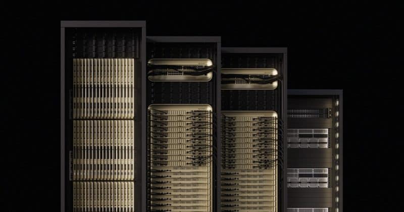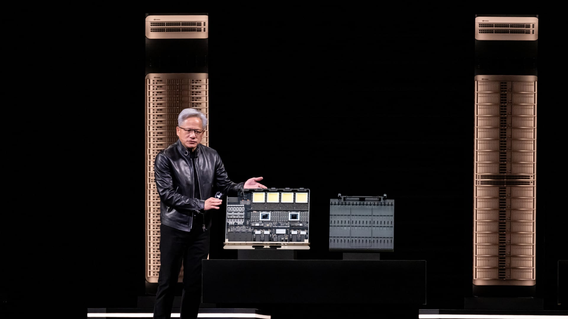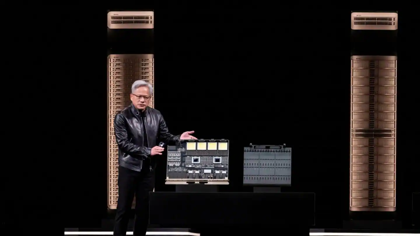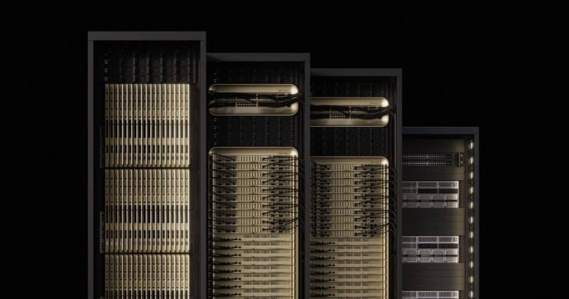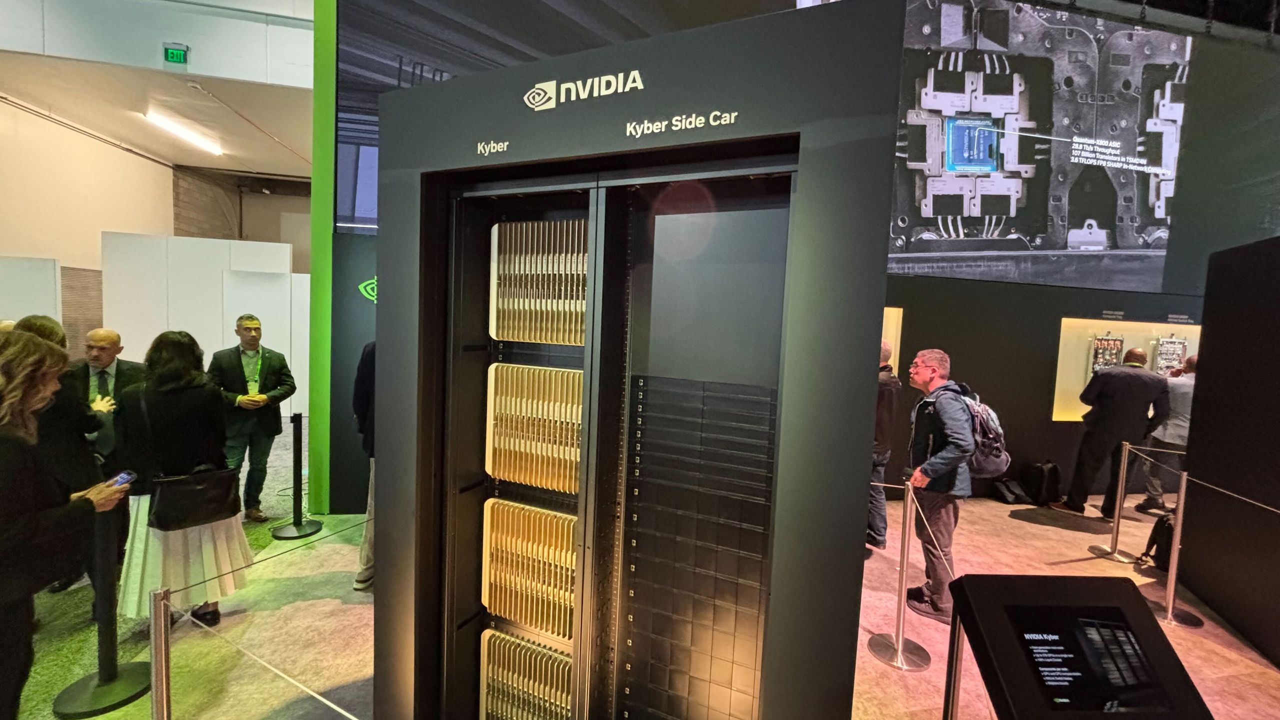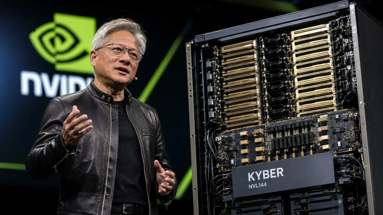
SemiAnalysis says Nvidia’s Kyber NVL144 rack system has slipped to 2028 because its PCB midplane remains difficult to manufacture. Nvidia has not publicly confirmed that date. The report does not establish that Nvidia’s Rubin GPU itself is late, but it raises a more awkward problem for the company: its next leap in AI computing depends on making 144 GPUs behave like one tightly connected machine, and the obstacle may sit in the rack rather than the chip.For AI labs, cloud providers and investors, that distinction matters. Nvidia can continue selling Rubin NVL72 systems if they arrive on the company’s stated schedule. But a delay to Kyber could leave a gap in Nvidia’s route to much larger all-to-all NVLink domains, at the same moment AMD, Google and AWS are building rival scale-up systems of their own. The story is not about a board holding up a server. It is about whether the AI industry’s next performance gains can still arrive as promised once chips, memory, switches, cooling, power and factory yield all have to work together.Key takeawaysThe reported Kyber problem is a rack-level manufacturing issue, not confirmed evidence of a Rubin GPU delay. SemiAnalysis points to the PCB midplane, while Nvidia still says Rubin is in production and partner systems are due in the second half of 2026.Kyber matters because it is supposed to double Nvidia’s NVLink scale-up domain per rack from 72 GPUs to 144. That matters most for workloads that spend large amounts of time moving model state, parameters and intermediate results between accelerators.AMD, Google and AWS have a sales opening, though none offers a simple drop-in replacement for Nvidia.AMD’s Helios, Google’s TPU 8t and AWS Trainium3 all give hyperscalers alternatives for large AI clusters or tightly connected accelerator systems.Nvidia’s counter is already visible: ship Rubin NVL72, push scale-out networking, sell specialised Rubin CPX systems, and turn hyperscalers’ custom chips into customers of NVLink through NVLink Fusion.TSMC is exposed differently. A PCB midplane delay would not be a direct failure of TSMC’s wafer fabrication or CoWoS packaging, but it strengthens customers’ arguments for more options in advanced packaging, where Intel Foundry and Samsung Foundry are seeking relevance.The report that has put Kyber under scrutinyCNBC’s report, citing SemiAnalysis, has put a sharp claim into the market: Nvidia’s Kyber NVL144 rack is reportedly delayed by more than a year, from an earlier 2027 expectation to 2028, because of manufacturing difficulties around its PCB midplane. SemiAnalysis also argues that Nvidia has cancelled an interim NVL72x2 design and may face separate limits in scaling NVL576 systems because co-packaged optics remain hard to deploy at volume. Those are material claims, but they remain SemiAnalysis reporting and analysis unless Nvidia, a system maker or a supplier confirms them.Nvidia’s public material still presents Kyber as the next-generation MGX NVL rack. In March, it said Kyber would double the NVLink domain per rack to 144 GPUs, then form the basis for an NVL1152 design that joins eight Kyber racks using direct optical interconnects. Nvidia described Kyber’s first appearance as a standalone NVL144 system associated with Vera Rubin Ultra.The company’s earlier power-infrastructure material also placed Kyber alongside 800 VDC AI data-centre designs in 2027. That makes SemiAnalysis’s 2028 claim significant even without an official Nvidia acknowledgement. A one-year shift in a rack-scale programme can affect customer data-centre construction schedules, power contracts, cooling plans and accelerator procurement well before any GPU leaves a factory.The central editorial discipline here is simple: Kyber is not Rubin. Rubin is Nvidia’s broader next-generation platform. Kyber is a proposed physical rack architecture and interconnect approach within Nvidia’s longer AI infrastructure plan. Nvidia says Vera Rubin is ramping into full production and that Rubin-based systems will be available from partners in the second half of 2026. A reported Kyber delay therefore need not stop Rubin NVL72 systems from reaching customers.That does not make the Kyber issue minor. It simply changes the question. The problem is not whether Nvidia can sell a new GPU generation. The problem is whether it can deliver the densest and most tightly connected version of that generation on the timing it had implied.What Kyber is trying to doFor years, Nvidia’s pitch has moved steadily away from the idea of a GPU as a standalone product. The company now sells an integrated machine: compute, switching, networking, storage interfaces, software libraries, liquid cooling, power distribution and management software assembled into one operating unit.Kyber is an attempt to push that integration further.Nvidia’s current Vera Rubin NVL72 architecture links 72 GPUs through sixth-generation NVLink and NVLink switches. Nvidia says NVLink 6 provides 3.6 TB/s of bidirectional GPU-to-GPU bandwidth, while the NVL72 can deliver 260 TB/s of aggregate scale-up bandwidth. In plain English, the aim is to allow every GPU in the rack to communicate with every other GPU quickly enough that software can treat the system more like one giant accelerator than 72 isolated machines.Kyber is meant to double that tightly coupled domain. Nvidia’s March roadmap says Kyber will hold 144 GPUs in one rack-scale NVLink domain, then help form larger all-to-all systems such as NVL1152. The company’s objective is not simply more GPUs in one room. It is to reduce the amount of time those GPUs spend waiting for one another.That wait matters.Large language models and reasoning systems do not run as one uninterrupted burst of arithmetic. Data moves between high-bandwidth memory, CPU memory, GPU memory, networking buffers and storage. Mixture-of-Experts models can route tokens between specialist sections of a model. Tensor parallelism splits one calculation across several accelerators. Long-context inference requires huge quantities of data to remain accessible while a model reads, retrieves and generates. If the communication path is slow, the GPUs sit idle. A rack with more theoretical FLOPS can then deliver less useful work than expected. Nvidia itself argues that current AI workloads are limited by sustained execution across compute, memory and communication, rather than by headline floating-point performance alone.The Kyber idea is therefore closer to rebuilding the service core of a high-rise than stacking another floor on top. A conventional rack can use extensive cabling to connect compute trays and switches. Kyber is designed to make the electrical route part of the building itself: vertical compute blades, switch blades at the rear, and a cable-free midplane that acts as the shared spine. It should create more room, reduce cable complexity and make a much denser arrangement possible. But if the building’s central spine cannot be manufactured consistently, the upper floors cannot open.Why a PCB midplane can become the limiting componentA PCB midplane is easy to underestimate because it looks less dramatic than a GPU package containing advanced logic dies and stacks of high-bandwidth memory. Yet a high-speed rack midplane is not an ordinary circuit board.In Kyber, it would have to connect a large number of compute blades and NVLink switch blades through short, precisely controlled electrical paths. At these data rates, every trace behaves less like a forgiving wire and more like a transmission line. Signal loss, reflections, crosstalk, impedance variation and timing mismatch can all become material. The faster the link, the smaller the margin for inconsistency. Nvidia’s own NVLink material makes clear that its sixth-generation fabric is designed for all-to-all communication at 3.6 TB/s per GPU. That is an extraordinary amount of traffic to sustain inside a physical rack.The engineering challenge becomes sharper when electrical design meets production reality.A board can work in a prototype and still fail the test that matters commercially: can a manufacturer make thousands of them at acceptable yield, with connectors lining up reliably, electrical performance staying within tolerance, and test procedures catching faults before a rack reaches a customer? SemiAnalysis’s claim is about manufacturability, which points towards this phase of the problem. A design may be technically sound but difficult to fabricate, inspect, assemble or qualify at volume.The midplane also has to coexist with Kyber’s broader physical design. Nvidia has described the rack as using vertically oriented compute blades, purpose-built switch blades, higher GPU density, liquid cooling and a shift towards 800 VDC power infrastructure. Each choice brings advantages. Each choice increases the number of interfaces that must hold their tolerances at the same time.Power is part of the complication. Nvidia’s proposed 800 VDC approach is intended to reduce the amount of electrical conversion happening near the rack, cut copper and component overhead, and make extremely dense AI systems more practical. The company says the architecture requires work on safety, standards and workforce training at the facility level. That is a reminder that a rack approaching megawatt-class power is no longer just an IT product. It is part server, part industrial electrical installation.Cooling is another part. Nvidia says its Rubin generation is designed around fully liquid-cooled infrastructure, with every chip and networking component in the system using liquid cooling. That can improve density and remove heat more effectively than air, but it adds cold plates, manifolds, quick disconnects, coolant distribution systems and leak-management requirements to the bill of materials.A Kyber delay, if confirmed, would show why the term “AI factory” is more than marketing. The chip is only one section of the machine. The rack must survive electrical testing, mechanical handling, thermal cycling, pressure management, field servicing and data-centre installation. Failure in any one section can stop the whole product.Copper inside the rack, light between the racksThe reported difficulty around Kyber sits beside a separate question: how Nvidia connects racks once one rack is no longer large enough.Nvidia’s NVL576 concept is built around eight racks with 72 Rubin Ultra GPUs each, joined into a 576-GPU NVLink domain through a two-layer topology using copper and direct optical links. The company says it has already demonstrated a functional GB200-based prototype of a multi-rack NVL576 architecture.Kyber’s future NVL1152 system is supposed to follow the same logic on a larger scale, using direct optical interconnects between racks. That is where SemiAnalysis has raised a second concern: the claim that co-packaged optics could delay or constrain larger systems. Nvidia has not confirmed that assessment.Co-packaged optics places optical engines close to the networking silicon rather than relying only on removable pluggable optical modules. The aim is lower power use, more bandwidth density and better signal quality at very high speeds. Nvidia is already promoting co-packaged optics in its Spectrum-6 Ethernet platform, which it says uses 200 Gb/s optical lanes and 102.4 Tb/s switch bandwidth for AI scale-out networks.The attraction is obvious. Electrical signals weaken as they travel over longer copper paths. Light can carry data over longer distances with less of that penalty. But shifting from copper to optics changes the engineering problem rather than abolishing it. Optical alignment, packaging, thermal management, fibre handling, repair procedures and manufacturing yield all matter. At rack scale, a technology can be elegant and still be commercially awkward until it is field-proven at large volumes.This is why Kyber’s alleged delay should be read as part of a wider transition. Nvidia is trying to move from scale-up systems that fit inside a rack to scale-up domains that span several racks and eventually several thousand GPUs. The technical barriers rise sharply because every additional layer multiplies the number of physical, electrical and operational dependencies.The roadmap gap Nvidia now has to manageThe useful way to read Nvidia’s roadmap is through the difference between what is officially stated and what remains reported.Product or designRole in Nvidia’s planPublic statusVera Rubin NVL7272-GPU NVLink rack-scale systemNvidia says Rubin is in production and partner systems will be available in H2 2026.Rubin CPXA specialised platform for massive-context inferenceNvidia has said Rubin CPX will be available at the end of 2026.Vera Rubin Ultra NVL576Eight racks combined into one 576-GPU NVLink domainNvidia has announced the design and shown a prototype architecture.Kyber NVL144New rack design meant to place 144 GPUs in one NVLink domainNvidia has described it as a future Vera Rubin Ultra system. SemiAnalysis says it has slipped to 2028.Kyber NVL1152Eight Kyber racks linked through direct optical interconnectsNvidia describes this as a later Feynman-era direction.The most important distinction is between Rubin CPX and Kyber NVL144. Both involve “144” in Nvidia’s broader product naming, but they are not automatically the same physical machine or the same market proposition.Rubin CPX is a specialised system designed around large-context inference tasks such as coding, video generation and workloads involving million-token-scale context windows. Nvidia has said it expects Rubin CPX to be available at the end of 2026.Kyber, by contrast, is a new rack architecture intended to double the NVLink domain per rack and later scale into larger all-to-all systems. A delay to Kyber would not erase Rubin CPX. It would affect Nvidia’s more ambitious route to making 144 GPUs function as one low-latency NVLink-connected unit, then extending that capability into much larger multi-rack domains.That leaves Nvidia with an obvious mitigation: sell more NVL72 systems.For many buyers, that may be enough. A cloud provider needing capacity for mainstream inference, AI coding tools, internal copilots, fine-tuning or large but conventional training runs can deploy several NVL72 racks and link them through Ethernet or InfiniBand. The practical compromise is that a larger cluster connected through a scale-out network does not always behave like a single 144-GPU or 576-GPU all-to-all domain. The communication path may involve more hops, more software orchestration and more exposure to network contention.The result is not “Nvidia has no answer”. The result is that customers who need the largest tightly coupled systems may have to decide whether to wait, redesign their workloads or choose a rival route.How Nvidia’s rivals can take advantageNvidia’s competitors have an opening because Kyber is a system-level product. The customer question is not simply “which company has the faster chip?” It is “which supplier can deliver a usable, supportable, power-ready AI cluster in the time window we have?”AMD has the most direct commercial opening.Its Helios platform is designed as a rack-scale alternative built around Instinct MI455X accelerators, EPYC “Venice” CPUs and Pensando networking. AMD says Helios can deliver up to 3 AI exaflops in a single rack and is designed for trillion-parameter model training. The platform is based on the Open Rack Wide specification contributed by Meta to the Open Compute Project, which gives AMD an “open” counter-position against Nvidia’s tightly controlled rack integration.AMD can now make a sharper procurement argument. A cloud operator that expected to build its 2027 plans around Kyber could spread risk by qualifying Helios alongside Nvidia’s systems. The pitch is not merely lower cost. It is optionality: do not let one supplier’s rack schedule decide your data-centre utilisation, power commitments and AI product roadmap.AMD’s limitation is equally clear. Helios itself is a new rack-scale platform with its own supply-chain and software qualifications to complete. AMD has said Helios systems are aimed at 2026 availability, but customers will still need to test real performance, ROCm maturity, networking behaviour and operational reliability at scale. Nvidia’s CUDA software position, OEM reach and installed base remain difficult to displace merely because a rival has a compelling block diagram.The India angle makes AMD more interesting than it might otherwise be. AMD and TCS have announced plans for a Helios-based AI infrastructure design in India, with a blueprint supporting up to 200 MW of AI-ready data-centre capacity through TCS subsidiary HyperVault. It is an announced plan, not a confirmed operational deployment, but it gives AMD a local route to present Helios as part of India’s sovereign-AI build-out rather than only as a Silicon Valley alternative to Nvidia.Google has a different advantage: it already operates its own cloud and can sell access to an alternative scale-up system without persuading customers to buy hardware.Google says TPU 8t uses a 3D torus interconnect across 9,600 chips in one Superpod, aimed at large-scale pre-training and embedding-heavy workloads. It also describes a Virgo network that can connect more than 134,000 TPU 8t chips in one fabric. These are Google claims, not independent benchmarks against Kyber. Still, they allow Google Cloud to tell frontier-model builders that the relevant scale question is not “can you fit 144 GPUs in one Nvidia rack?” but “can you deliver thousands of accelerators with predictable training performance?”Google’s constraint is software and business model. TPU customers must adopt Google Cloud’s hardware platform, compiler stack and operational model. That can work well for organisations prepared to build around JAX, XLA and Google’s managed infrastructure. It is less attractive for buyers whose software, talent and procurement processes are built around CUDA and Nvidia’s server ecosystem.AWS has an opening too, but its relationship with Nvidia is more complicated.AWS’s Trainium3 UltraServer scales up to 144 Trainium3 chips and uses NeuronSwitch-v1 as an all-to-all fabric. AWS says the system can scale into UltraClusters containing hundreds of thousands of chips, while targeting reasoning, Mixture-of-Experts, reinforcement learning and long-context workloads. That makes Trainium3 a useful alternative for buyers who want 144 accelerators in a tightly connected system without waiting for Kyber.Yet AWS is not simply taking customers away from Nvidia. It has also agreed to use Nvidia NVLink Fusion in the future Trainium4 generation. Nvidia says AWS is designing Trainium4 to integrate NVLink 6 and the MGX rack architecture, allowing AWS’s custom chips, Graviton CPUs, Elastic Fabric Adapters and Nitro virtualisation technology to sit inside a Nvidia-derived rack-scale foundation.That agreement reveals Nvidia’s strategic answer to custom silicon. Nvidia does not need every accelerator sold by a hyperscaler to be an Nvidia GPU. It can still retain a valuable role if the hyperscaler uses Nvidia networking, switch technology, rack architecture and supplier relationships. In the AI infrastructure market, control of the interconnect can be almost as valuable as control of the compute die.Broadcom and other custom-chip partners could also benefit indirectly. A Kyber delay gives hyperscalers another reason to spend on in-house accelerators and Ethernet-based AI fabrics, particularly for workloads they understand well enough to optimise in-house. The catch is that custom silicon does not remove the rack problem. It transfers it. A company building its own accelerator still has to solve power, cooling, networking, software, manufacturing and serviceability. Nvidia’s NVLink Fusion pitch exists because those steps cost billions of dollars and can consume years.Nvidia’s counterplay is broader than one rackNvidia has several ways to limit the impact of a Kyber delay.The obvious one is volume. Rubin NVL72 remains the company’s main near-term rack-scale product, and Nvidia says Rubin is already in full production. The company has named AWS, Google Cloud, Microsoft, Oracle Cloud Infrastructure, CoreWeave, Lambda, Nebius and Nscale among the early cloud providers expected to deploy Rubin-based instances in 2026.That gives Nvidia a large commercial buffer. A buyer that wants a 72-GPU NVLink domain, CUDA compatibility and access through major clouds does not need Kyber to begin deploying Rubin-era systems. Nvidia can keep revenue flowing through NVL72 while it works through any Kyber manufacturing problem.The second counter is product segmentation. Rubin CPX gives Nvidia a 144-GPU offering aimed at massive-context inference from the end of 2026, according to the company’s stated schedule. It does not solve every use case addressed by Kyber, but it offers Nvidia another path to tell buyers that the “144 GPU” number is not disappearing from its product portfolio.The third counter is scale-out networking. Nvidia’s Spectrum-X Ethernet and Quantum-X InfiniBand systems allow customers to build bigger clusters from available racks. Scale-out is less elegant than an enormous single all-to-all NVLink domain for some jobs, but it is a valid answer for workloads that can be partitioned efficiently. Nvidia’s own Rubin material treats the data centre as a collection of specialised racks linked through scale-up and scale-out fabrics rather than a single monolithic machine.The fourth is NVLink Fusion. This is the more strategically important response because it changes Nvidia’s role from component supplier to rack-platform provider. The company says NVLink Fusion can connect up to 72 custom ASICs all-to-all at 3.6 TB/s per ASIC and provides customers access to MGX rack designs, networking, liquid cooling, power components and software.That approach also protects Nvidia from a future in which AWS, Google, Microsoft and Meta buy fewer Nvidia GPUs but more of their own accelerators. Nvidia can still sell the roads, switches and construction rules of the AI factory.The limitation is unavoidable. None of these measures changes the fact that Kyber’s core promise is physical density plus a larger scale-up domain inside one rack. More NVL72 systems can offset compute capacity. They cannot fully substitute for a 144-GPU all-to-all domain where a customer’s workload genuinely benefits from it.What this means for TSMC, Samsung and Intel FoundryTSMC’s position in this story is more indirect than some headlines imply.The reported Kyber bottleneck is a PCB midplane. That is a rack-level interconnect component. It is not the same thing as a GPU wafer, a high-bandwidth memory stack or TSMC’s CoWoS advanced packaging process. There is no evidence in the SemiAnalysis claim that TSMC’s core production of Rubin chips is the direct cause of the alleged Kyber delay.TSMC still has its own hard problems. Its chairman, C.C. Wei, said in the company’s April earnings call that advanced packaging capacity remained tight. TSMC also acknowledged customer demand for ever-larger reticle-size packages, competition from Intel’s EMIB approach and technical pressures involving mechanical stress, warpage and thermal limits.That is the broader point. AI systems are moving into a period where packaging, substrate size, memory integration and mechanical behaviour become as commercially important as transistor density.TSMC’s answer is to keep extending its advanced packaging capabilities and add capacity. On the earnings call, the company said it was working on larger reticle-size packaging and CoPoS, while continuing to expand its high-end packaging capacity. It also said that its leading advanced-packaging capacity was tight, which illustrates why customers have begun looking more seriously at alternatives.Intel Foundry has a credible way into that conversation. Its EMIB technology uses embedded bridges to link multiple dies, while Foveros Direct uses copper-to-copper hybrid bonding for dense 3D stacking. Intel presents EMIB and Foveros as options for data-centre and AI designs requiring heterogeneous integration across different chiplets and process technologies.Samsung Foundry is taking a similar position through its Cube-S and other heterogeneous-integration offerings. Samsung says 2. 5D Cube-S places logic and HBM dies on a silicon interposer to create high-bandwidth, low-latency links, while its packaging portfolio also includes vertically stacked approaches intended to shorten interconnects and manage larger multi-die systems.Neither Intel nor Samsung can solve a Kyber PCB problem merely by winning a package order. That would be a category error. Their chance lies elsewhere: a report exposing the fragility of one AI supply chain can make customers more willing to qualify several foundry, packaging and HBM routes for future chips.For TSMC, the response cannot be limited to saying that its wafers are ahead. It must keep proving that it can supply the largest, most difficult packages at volume, manage capacity constraints and stay close enough to customers that rival packaging approaches do not become a strategic hedge.Nvidia faces the rack challenge. TSMC faces the diversification argument. They are linked, but not interchangeable.Taiwan’s role: central, but not the whole explanationTaiwan remains the physical centre of Nvidia’s AI hardware production. Nvidia says its Vera Rubin systems are being manufactured at scale by Taiwanese server makers and supply-chain partners, including companies such as Foxconn, Quanta, Pegatron, Wistron and Inventec.That concentration is an advantage. Taiwan has deep experience across advanced chip fabrication, packaging, substrates, boards, server assembly, liquid cooling, power electronics and final system integration. Nvidia’s ability to move from a GPU design to a rack-scale product depends heavily on that industrial depth.It also produces a harder operational reality. A leading AI rack is not manufactured by one company in one factory. It is assembled through many specialised suppliers, each working to demanding electrical, thermal and mechanical tolerances. A delay in a PCB midplane can slow a product even when the GPU package, HBM memory, switch silicon and server chassis are otherwise ready.The accurate conclusion is not that “Taiwan manufacturing has failed”. It is that AI racks have become so complex that one difficult component in a Taiwan-centred supply chain can constrain the launch of a global product. That is a much more specific and useful explanation.Why India should care, even without a Kyber order bookThere is no public confirmation that Kyber systems are headed to India, and no public Indian delivery schedule for the rack. That limits the immediate direct effect.India’s nearer AI-compute story is likely to be shaped by cloud availability, local data-centre construction, power access, sovereign-AI procurement and the price of accelerator capacity. Nvidia’s Rubin NVL72 is expected to appear through major cloud providers later in 2026, while Google Cloud has said its A5X offering will use Vera Rubin NVL72 once the platform becomes available.A Kyber delay could still matter indirectly. If the largest global AI labs and cloud providers cannot receive the rack-scale systems they planned for 2027, they may keep more capacity tied up in earlier-generation systems, extend contracts for existing GPU clusters or compete harder for available Rubin NVL72 inventory. That can affect global cloud pricing and lead times, including for Indian startups and enterprises buying AI infrastructure through international providers.AMD’s TCS partnership makes the competitive dimension more concrete in India. The two companies say they will co-develop a Helios-based AI infrastructure design supporting up to 200 MW of capacity. Whether that becomes operational at the promised pace will matter more to Indian buyers than an abstract comparison of Nvidia and AMD peak specifications. The real test will be power availability, data-centre execution, software support, customer access and cost per useful training or inference job.That is the wider lesson of Kyber. India does not need to wait for a 144-GPU Nvidia rack to build useful AI capacity. But it does need to understand that the frontier of AI infrastructure has moved beyond buying chips. Power, cooling, network design, manufacturing schedules and operational skill now determine who can turn hardware into usable compute.What to watch nextThe next evidence will not necessarily come from Nvidia first.Watch Nvidia’s earnings calls and product-roadmap language. A continued reference to 2027 Kyber deployment would challenge SemiAnalysis’s reported timetable. A shift towards more Rubin NVL72 volume, Rubin CPX capacity or later Feynman timing would support the idea that the company is filling a hole in its roadmap.Watch Nvidia’s OEM partners. Foxconn, Quanta, Wistron, Pegatron, Dell, HPE, Supermicro and other system suppliers often reveal the pace of qualification and delivery through their own announcements before end customers see the racks.Watch whether Nvidia says more about NVL576. A successful transition from NVL72 to a multi-rack 576-GPU NVLink domain would reduce the commercial impact of a Kyber delay. Continued silence or a move towards small-volume deployments would make the SemiAnalysis warning more credible.Watch co-packaged optics. Nvidia is publicly investing in it for scale-out Ethernet and future larger systems. The question is whether the technology can move from engineering promise to routine, serviceable deployment at the scale hyperscalers require.Watch customers. A major Helios order, more TPU commitments, larger Trainium deployments or a rise in custom-silicon spending would show that the reported delay is changing procurement decisions. That matters more than a roadmap slide.The real significance of the Kyber reportThe Kyber report is important because it exposes the part of the AI race that chip charts tend to hide.For more than a decade, the semiconductor industry could discuss progress through nodes, transistor counts, memory bandwidth and TOPS. Those figures still matter. But AI systems are now hitting another frontier: the difficulty of turning individually impressive components into one manufacturable machine.Nvidia’s argument is that the data centre, not the GPU, is the unit of compute. Kyber is the consequence of taking that idea seriously. It tries to combine 144 GPUs, high-speed switching, liquid cooling, extreme power density and a dense rack layout into one operational product. The prize is substantial. The risk is that the hardest work moves from silicon design into the areas where yield, tolerances, connectors, servicing and factory repetition decide what can actually ship.SemiAnalysis may ultimately be proved right about a 2028 Kyber arrival. Nvidia may find a workaround, redesign the midplane, adjust the configuration or show that the report overstated the delay. The public evidence does not yet settle that question.What is already clear is that Nvidia’s rivals now have an opening to sell something more valuable than a faster chip: certainty. AMD can sell an alternative rack path. Google can sell giant TPU systems through its cloud. AWS can offer Trainium3 while tying Trainium4 partly back to Nvidia’s network technology. Intel and Samsung can press customers to qualify more advanced-packaging options. Nvidia can counter with Rubin NVL72, Rubin CPX, scale-out networking and NVLink Fusion.The fight has moved from the die to the whole machine.FAQ: Nvidia Kyber delay explainedIs Nvidia Kyber delayed to 2028?SemiAnalysis says Kyber NVL144 has been delayed to 2028 because of difficulty manufacturing its PCB midplane. Nvidia has not publicly confirmed the date in the product material cited here, so the 2028 timetable should be treated as reported rather than confirmed.Does the Kyber report mean Nvidia Rubin GPUs are delayed?Not on the evidence available. Nvidia says Vera Rubin is ramping into full production and that Rubin-based partner systems will be available in the second half of 2026. Kyber is a later rack-scale architecture built around a larger NVLink domain.Why does a PCB midplane matter for AI performance?The midplane is meant to connect compute and switch blades through short, high-speed electrical paths inside the rack. If those links cannot be produced reliably, Nvidia cannot deliver the physical design needed to make 144 GPUs operate as one all-to-all NVLink domain. That affects workloads where communication between accelerators is a major source of delay.Can Nvidia simply connect two 72-GPU racks instead?It can connect many NVL72 racks through scale-out networks such as Ethernet or InfiniBand. That adds total capacity, but it may not provide the same latency, bandwidth consistency or all-to-all communication characteristics as a single 144-GPU NVLink domain.Which companies could gain if Kyber is delayed?AMD has a direct opening with Helios; AWS can promote Trainium3 UltraServers; Google can sell TPU 8t capacity through Google Cloud; and custom-silicon suppliers gain another argument for diversification. Intel Foundry and Samsung Foundry benefit more indirectly, through a stronger case for alternative advanced-packaging routes.end of article
Nvidia Kyber delay: why a circuit board could alter the AI infrastructure race
Is Nvidia’s Kyber rack delayed, and what does it mean for the AI infrastructure market?
4,999 words~23 min read