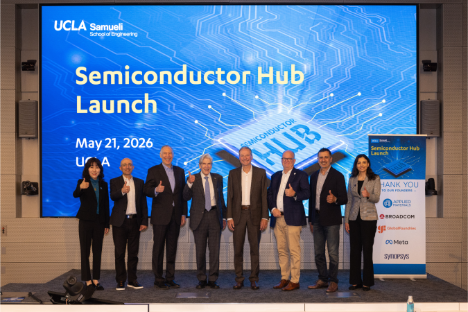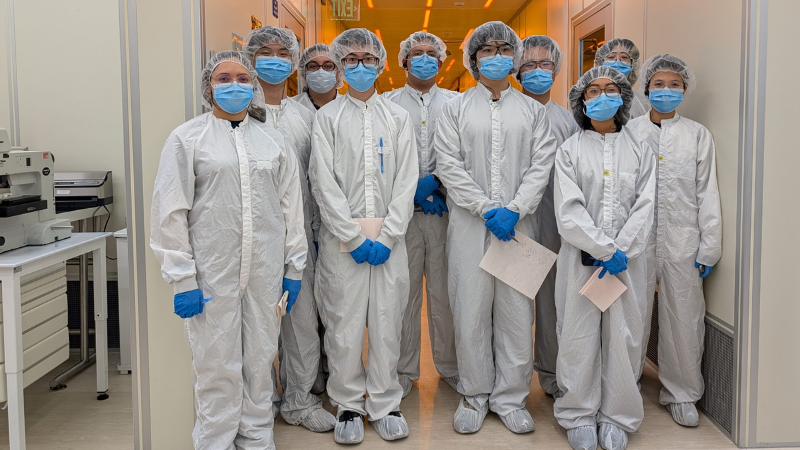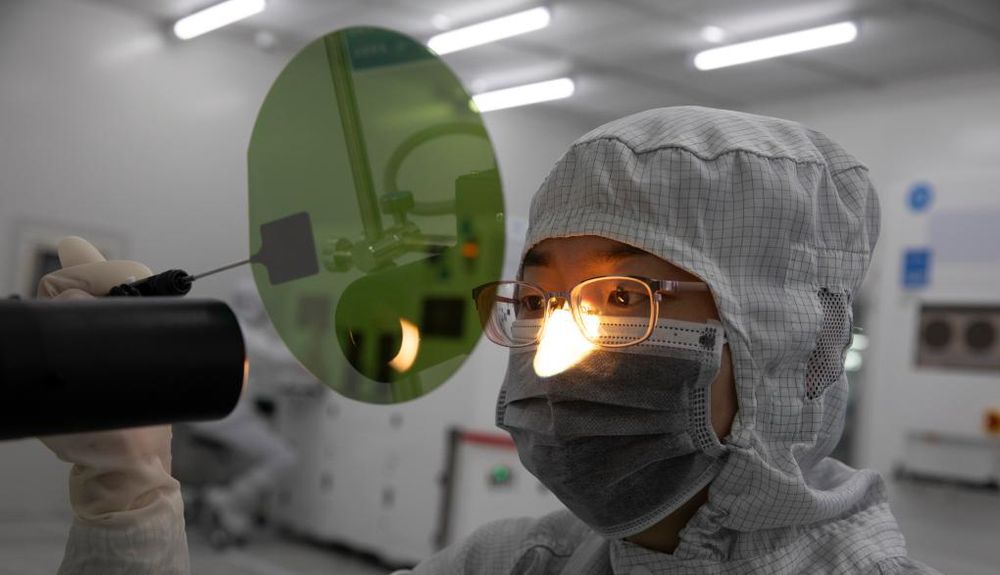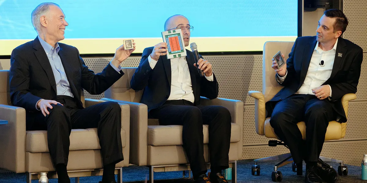
Semiconductor companies and universities are trying to shorten their feedback loop to meet the challenges of the AI era. In recent years, National Yang-Ming Chiao Tung University in Taiwan, the University of California, Berkeley, Arizona State University, Virginia Tech, and others have been building closer links with industrial partners, as both sides seek to speed turning research into business, and inform the next round of research with fresh lessons from industry.Now, the University of California, Los Angeles, and five major semiconductor companies announced in May a new US $125 million university-industry hub that takes that idea and runs with it.Chip packages are growing larger and more complex as manufacturers scramble to keep up with the memory and processing demands of today’s frontier AI models. Frontier models undergo step-change updates every few months, compared to semiconductor parts, whose manufacturers typically update on an 18- to 48-month cycle, depending on the particular component. As a result, demand for AI-capable processors has outpaced production capacity, and prices for components at the chokepoints are spiking.UCLA’s Semiconductor Hub includes partners at each stage of the semiconductor manufacturing process, spanning materials, architectural design, tooling, packaging, and fabrication. The work will address communications systems and AI inference at network edges—meaning in peripheral devices far from central servers. Bridging University Research and Chip FabsThe need for a stronger bridge from university to semiconductor fabs is clear. In February, Purdue University and Imec researchers wrote in Nature Reviews Electrical Engineering that the semiconductor industry was going to need a wider funnel of ideas to keep up with the complexities of 2D materials, enormous silicon wafers, and the tremendous demand from the AI industry. They called for more reliable, industry-ready research labs that would help transfer successful university prototypes into reliable, well-documented materials companies could build at larger scale. Universities should train and retain skilled technical workers at the interface of semiconductor research and commercialization so they can address industry needs, the authors wrote.There is now so much research to do, spanning so many different specialties, at the bleeding edge of semiconductor innovation that it is the rare company that can afford to go alone, said Gary Dickerson, the president and CEO of Applied Materials, at the hub’s launch. “The companies that are doing the best in semiconductors are those that have been best at collaborating.”With the UCLA hub, that collaboration now includes even more with academia. The UCLA hub will also adopt a flexible approach to problem-solving and career integration between academia and industry. The hub’s leadership will encourage participating faculty to pivot research projects on faster timescales than conventional federal funding allows, says Ah-Hyung “Alissa” Park, dean of the UCLA Samueli School of Engineering. Doctoral students, who will be co-advised by academic and industry supervisors, will also spend a year in industry internships in their fourth year.The industry partners include Applied Materials, GlobalFoundries, Meta, Synopsis, and Broadcom, whose founder, Henry Samueli, spun off the company from his research at UCLA in 1991. In some ways, the hub represents a doubling-down on that and other related relationships. “Many of our faculty are already working with this hub,” says Park.UCLA Semiconductor Hub Research FocusThe nearest parallel hubs in the U.S. are perhaps the Berkeley and Phoenix hubs, but they are each specialized in different stages of the semiconductor manufacturing process, and weighted toward industry. The UCLA program aims to address each phase of manufacturing, albeit from an earlier, blue-sky research stage. “Ours is very different because it is research-focused while collaborating with industry,” says Mona Jarrahi, a UCLA professor and the Semiconductor Hub’s faculty director.These companies have been accustomed to selling products that emerged from lab work 10 or 20 years before and are now trying to speed up the commercialization timelines to suit an era of more advanced robotics and AI. “A lot of tech is now in commercialization in two to three years,” Park says. If the UCLA Semiconductor Hub and similar university-industry bridges succeed, Ph.D. students of the future may see semiconductor projects they worked on reach commercial reality before they complete their doctorates.This story was updated on 2 July 2026 to correct the mistaken statement that Samueli approached UCLA about founding the hub. Park proposed the idea to Samueli.
UCLA’s Semiconductor Hub Is Rewiring Industry and Academia for AI
UCLA’s semiconductor hub tightens the academia-industry feedback loop
703 words~3 min read