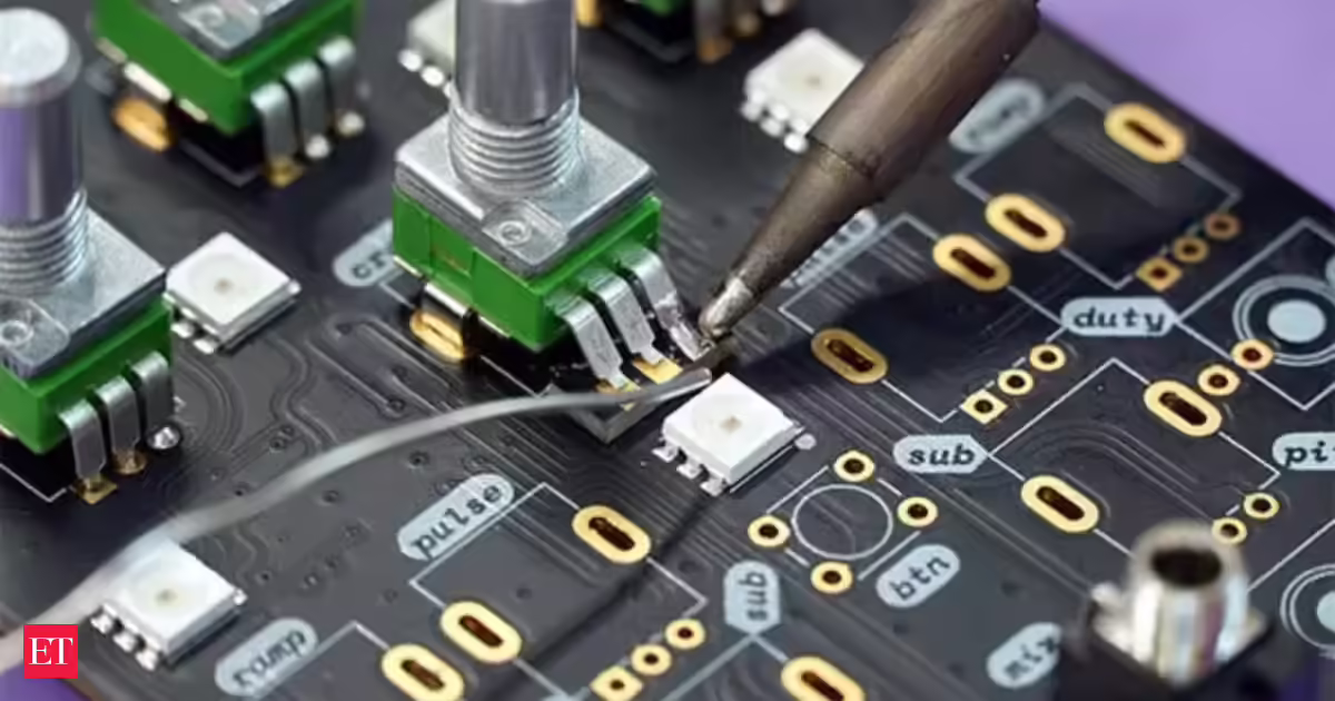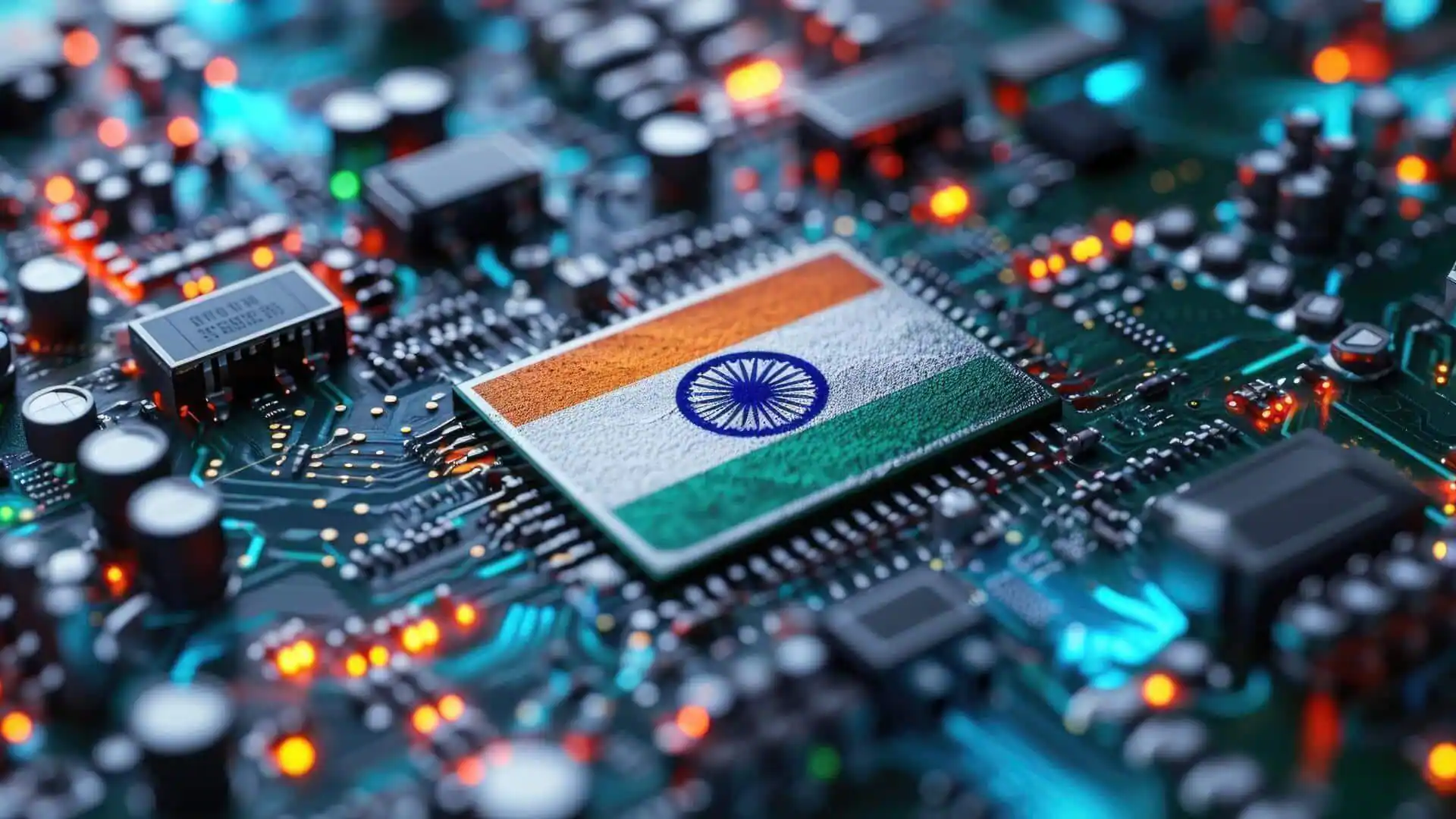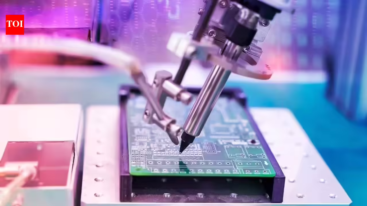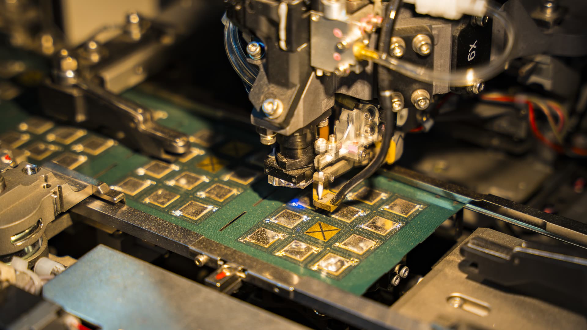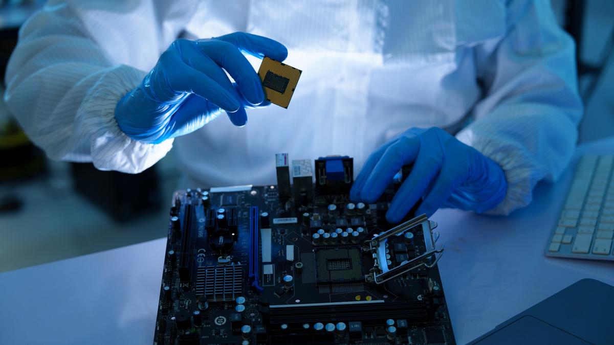
India’s Semiconductor journey is no longer just an aspiration, it is supported by real infrastructure, real capital and real policy intent. According to estimates by the Ministry of Electronics and Information Technology (MeitY), companies approved under the Indian Semiconductor Mission (ISM) are expected to invest nearly INR 312.99 billion by 2027. With such investments, India is positioning itself as a serious node in the global chip race. Manufacturing capacity alone will not determine if this ambition would translate into a self-sustaining ecosystem. Industry-level skilled talent is still one of the biggest challenges in India’s semicon journey.(Sign up for THEdge, The Hindu’s weekly education newsletter.)Union Minister Ashwini Vaishnaw has flagged a projected shortfall of one million semiconductor professionals globally, spanning fabrication, packaging, chip design, and testing. However, can traditional learning approach alone prepare the engineers needed for such complex and evolving industry? While Indian institutes produce large numbers of graduates, most lack hands-on exposure. As a result, a significant gap exists between academic learning and industry requirements.
Upcoming webinar: Is India a literate country?This is where technology innovation hubs become critical part of infrastructure. They close the gap between academic research which generates ideas, and industry, which needs deployable, actionable solutions. Facilities like Centre of Excellence (CoEs) and Incubation centres provide a common platform for mentorship, and industry exposure needed to transform ideas and talent skilling. Without this bridge, even the best research risks dying on the lab bench, and even the most advanced fabs risk running short of industry-ready engineers.Where ideas become chipsWith the continued expansion of the industry, innovation hubs and industry-academy collaboration are playing a crucial role in bridging the gap between education, research, and real-world semiconductor development. Institutions like IITs and IISc have been supporting thousands of students through tailored Master’s programs in semiconductor fabrication, process engineering and packaging among other.For instance, Centres of Excellence (CoEs) work closely with industry partners to ensure students develop skills that align with real-world needs, from chip design and fabrication to testing, packaging, and emerging technologies such as gallium nitride (GaN), and advanced semiconductor packaging. Several semiconductor Centres of Excellence, particularly in areas such as advanced packaging, GaN, and photonics, require government support given the significant capital they needed to build and sustain such infrastructure. These facilities can act as anchor hubs for both talent development and innovation, providing startups with access to pilot production, testing, and validation capabilities.The impact of such ecosystems is already visible, with IISc CeNSE alone developing more than 20 unique technologies in 2025. Another key example is Incubation Centres, they help transforming promising ideas into market-ready products and businesses. With India’s incubation ecosystem now comprising more than 1,100 active incubators, these centres provide startups with mentorship, funding access, industry connections, and shared infrastructure, making it easier for founders to navigate the long and capital-intensive journey of deep-tech innovation. Building these connections will not only strengthen the talent pipeline but also ensure that more research-led innovations successfully reach the market and contribute to India’s semiconductor ecosystem.Why this is critical to India’s chip ambitionsAs countries are investing heavily in semiconductor industry, skilled talent has become just as important as infrastructure and funding. For India, building a strong talent pipeline is critical to reduce foreign dependence on chip imports while strengthening its position across advanced research, chip design, manufacturing, packaging, and testing. The goal is not only to meet domestic demand but also to create a skilled workforce that can drive innovation and help in making India as a major semiconductor hubTo achieve this, India needs to expand their innovation hubs across more universities and regions, ensuring opportunities are available beyond the metro cities through which startups can access affordable labs and infrastructure. Industry must also play a larger role by helping design curricula, providing hands-on training, and investing in research infrastructure, which also helps startups connect with partners and potential customers more quickly. At the same time, stronger incubation support will be needed to help researchers and entrepreneurs turn ideas into successful businesses.India’s semiconductor ambitions will depend not only on building fabrication plants and manufacturing facilities but also on developing the talent and innovation ecosystem that supports them. Centres of Excellence and incubation centres are central to this effort, helping create skilled engineers, researchers, and entrepreneurs. The investments made in talent development today will play a key role in determining India’s competitiveness in the global semiconductor industry in the years ahead.(Co-authored by Srinivasan Raghvan, Professor at Centre for Nano Science and Engineering, IISc and Co-founder & Director at AGNIT Semiconductors, and Hareesh Chandrasekar, CEO & Co-Founder at AGNIT Semiconductors)