The company that packages and tests more semiconductors than anyone else on the planet just announced it’s building out 15 new facilities across Taiwan and Malaysia. ASE Technology Holding, which quietly sits at the heart of nearly every major chip supply chain, is scaling up to meet AI demand that shows no signs of slowing through at least 2029.
The expansion plan
Of the 15 new sites, six will be brand new ASE facilities, seven are designated for its subsidiary Siliconware Precision Industries (SPIL), and additional locations were acquired from display maker Innolux earlier this year. The geographic footprint spans Taiwan and Malaysia, two regions that already serve as critical nodes in the global semiconductor manufacturing network.
The buildout isn’t cheap. ASE has directed NT$17.8 billion toward a new facility in Kaohsiung’s Nanzih Technology Industrial Park alone, with that site slated for completion in the second quarter of 2028. For context, that single investment is roughly $550 million at current exchange rates, and it’s just one piece of a much larger puzzle.
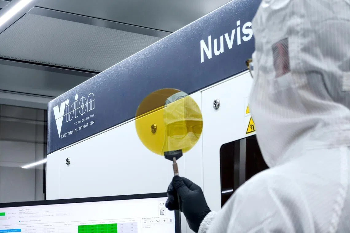
ASE’s suite of advanced packaging solutions, including its proprietary LEAP (Low-cost, Efficient, Advanced Packaging) platform, VIPack technology, and various other innovative methods, are precisely what hyperscale cloud providers and AI chip designers need. The company has revised its LEAP services revenue target for 2026 upward to over $3.5 billion, from an earlier estimate of $3.2 billion.