Home
Storia in 1 fonti
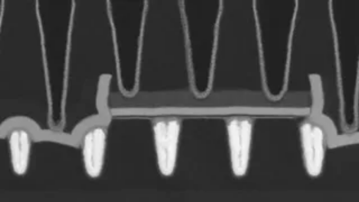
Post-silicon era gets closer as industry giants crack the 2D transistor scaling bottleneck with breakthrough tech — imec, ASML, and TSMC fab complementary 2D-material transistors at 50nm pitch on a 300mm wafer
EUV-printed 28nm gates and 94% working devices, all on standard production tooling.
Raccontata da tomshardware.com